
Luigi Ghezzi, Technical Marketing Engineer at Hamamatsu rounds up some of the most common applications for distance image sensors, and advises how to choose exactly the right distance image sensor.
Distance image sensors are image sensors that measure the distance to the target object using the Indirect TOF (time-of-flight) method. Used in combination with a pulse modulated light source, these sensors output delay time signals according to the timing in which the light is emitted and received. The sensor signals are arithmetically processed by an external signal processing circuit or a PC to obtain distance data.
For distance imaging, we can also use a standard image sensor, however, it usually takes a microsecond to perform the charge transfer from the photosensitive area to the storage section. Hamamatsu’s distance image sensors can make the transfer in the order of tens of nanoseconds. Other key features of our distance image sensors are:
- Drive voltage 5V or less
- Reduced effect of background light
- Compact chip size package (CSP) type
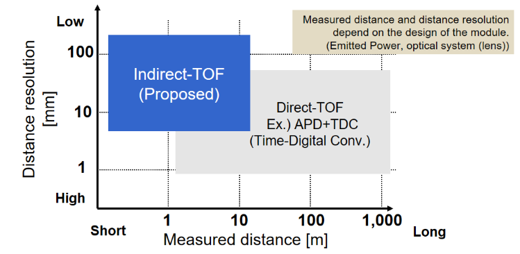
Distance image sensors are the best solution for the measurement range of 20 m, with a distance resolution of a few centimetres, for other distances, sensors such as APD+TDC are recommended.
Figure 1: Indirect-TOF and Direct-TOF - comparison of distance resolution and measured distance
Some example applications for distance image sensors are:
- Obstacle detection (self-driving, robot, etc.)
- Security (surveillance camera, intrusion detection, etc.)
- Factory automation (shape recognition, logistics, robots, object size, etc.)
- Motion capture, gesture
- Touchless operation (Air conditioner, automatic door, etc.)
Distance image sensor structure
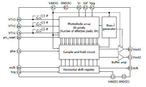
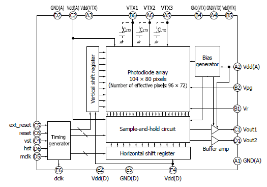
Hamamatsu can provide linear and area distance image sensors. Compared to a typical CMOS image sensor, the distance image sensor features:
- Pixel structure that allows high-speed charge transfer.
- The voltage needed to calculate the distance is output from two terminals.
Figure 2: Block diagram of linear and area distance image sensors
LINEAR AREA
The distance image sensors have a pixel structure in which electrodes are formed on local oxidation of silicon (LOCOS), so they generate a fringe electric field like CCD image sensors.
Figure 3: Pixel lateral surface potential
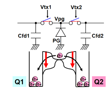
To obtain a high-speed charge transfer we use a pixel’s lateral surface potential to perform charge transfer and separation of the generated photoelectrons. In Figure 4 you can see the pixel structure.
Figure 4: Pixel structure
In the first phase, the potential profile sloping down towards VFD1 results in electric fields that quickly transfer the generated photoelectrons during this phase from their generation site under this PG to VFD1 through gate VTx1. The same mechanism transfers photoelectrons to node VFD2 in phase 2.
The measurement range is calculated by each photoelectron (Q1 and Q2). As result we have realized high-speed charge transfer.
The number of electrons generated in each pulse emission is several e-. Therefore, the operation shown in Figure 4 is repeated several thousand to several tens of thousands of times, and then the accumulated charge is read out. The number of repetitions depends on the incident light level and the required accuracy of distance measurement.
Indirect TOF (time-of-flight)
As previously mentioned, distance image sensors are based on the Indirect ToF method. In general, the ToF method calculates the distance by calculating the length of time for a light pulse travel from the light source, be reflected off an object, and return to the sensor.
Figure 5: Configuration example direct ToF Method
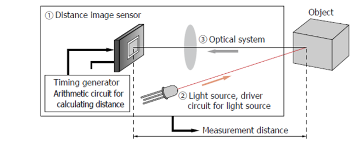
Figure 5 describes the direct ToF method. When we consider the phase difference information of light emitted and received, we are using the Indirect ToF method. In this method the charge generated in the photosensitive area is transferred to the storage section synchronously with the pulse of the light source, and the distance is calculated from the integrated charge.
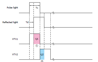
Figure 6: Basic principle indirect ToF Method
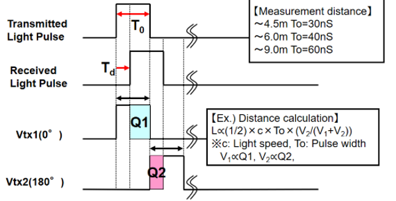
Pulses Vtx1 and Vtx2 are used to transfer generated electrons to two capacitance nodes (Vfd1 and Vfd2). From the accumulated charges in Q1 and Q2, and applying charge-to-voltage conversion, we obtain the output voltage Vout1 and Vout2:
Vout1 = Q1/Cfd1 = N x Iph x [(To-Td)/Cfd1]
Vout2 = Q2/Cfd2 = N x Iph x (Td/Cfd2)
Where:
Cfd1, Cfd2 are the integration capacitance of each output
N is the charge transfer clock count
Iph is the photocurrent
To is the pulse width of output light
Td is the delay time
From the previous formula, when Cfd1 = Cfd2, we can easily obtain the delay time:
Td = [Vout2/(Vout1+Vout2)] x T0
And using the output values (Vout1, Vout2) according to the distance D, expressed by the formula:
D = ½ x c x Td = ½ x c x [Vout2(/(Vout1 + Vout2)] x T0
For all distance measurements, ambient light is a key factor. In the indirect ToF method we use the difference between the output voltages, so the distance can be measured when background light is present.
Figure 6: Signal charge and background light charge
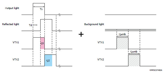
Figure 7: Integrated charge when background light is incident
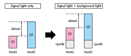
However, if the charge generated by background is large it can impact the saturation of the integration capacitance and narrow the dynamic range. For this reason, our distance Image sensors are equipped with a background elimination circuit.
Figure 8: Background light elimination circuit
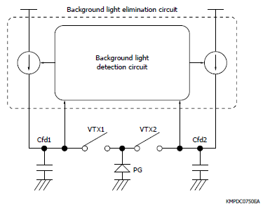
This background light detection circuit automatically operates when the output voltage approaches saturation. We denote the current caused by the signal light flowing through Cf1 and Cf2 as Iac1 and Iac2 and the current caused by background light as Iamb, but just to highlight the contribution of external light and to show how we can delete it. Remember that the charges caused by Iac1, Iac2 and Iamb are not distinguished, and they are integrated simultaneously. For this reason we denote the current caused by the incident light (signal light + background light) flowing through Cfd1 and Cfd2 as Iph1 and Iph2.
Figure 9: Background elimination circuit off
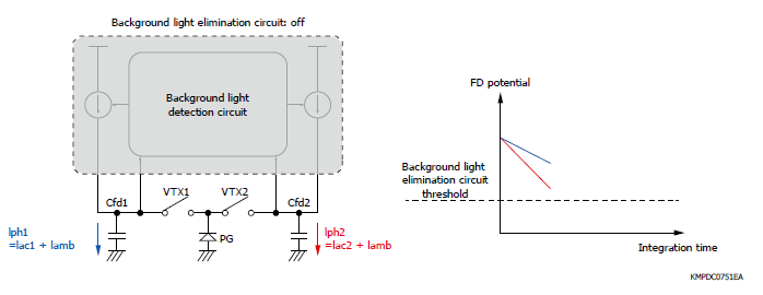
When the output voltage does not exceed the threshold, the circuit is off, and the background light is deleted from the ΔVout. From a numerical point of view we have:
Δvout1 = (Q1+Qamb)/Cfd1 = N x {[Iac1 x (T0-Td)]+(Iamb x T0 )}/Cfd1]
Δvout2 = (Q2+Qamb)/Cfd2 = N x {(Iac 2 x Td)]+(Iamb x T0 )}/Cfd2]
When the integration capacitance Cf1 and Cf2 are equal Δvout. Is:
Δvout= Δvout1 – Δvout2 = N x {[Iac1 x (T0 – Td)]- (Iac2 x Td)}/(Cf1 or Cf2)
As seen from the previous formula ΔVout is independent from Qamb (caused by the background light).
When one of the output voltages Vout1 or Vout2 exceed the threshold, the background circuit is activated and the larger of the two currents Iph1 and Iph2 is fed through Cfd1 and Cfd2. In the Figure 11 below, we will suppose that Iph1 is less than Iph2 so Iph2 is fed. In this situation the change in Vout2 is zero because the incoming current is equal to the outgoing current, and the electric potential is equal to the threshold of the background light elimination circuit. In the meantime, Cfd1 accumulates charge corresponding to Iph1-Iph2 and consequently Vout1 increases.
Figure 11: Background light elimination circuit: after operation (Iph1 <Iph2)
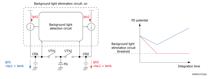
After the operation of the background light elimination circuit, we can describe ΔVout1 and ΔVout2 as:
ΔVout1 = [(Q1 + Qamb) – (Q2 + Qamb)]/Cf1 = (Q1-Q2)/Cf1=
= N x {[Iac1 x (T0-Td)+Iamb x T0]- [(Iac2 x Td) + (Iamb x T0)]}/Cf1=
N x {[Iac1 x (T0-Td)] - (Iac2 x Td) }/Cf1
ΔVout2 = [(Q2 + Qamb) – (Q2 + Qamb)]/Cfd2 = 0
When Cfd1 = Cfd2:
ΔVout= ΔVout1 - ΔVout2 = N x {[Iac1 x (T0 – Td)]- (Iac2 x Td)}/(Cf1 or Cf2)
Therefore, in this case, thanks to the operation of the background light elimination circuit, ΔVout is independent from Qamb (caused by the background light).
Additional features of Hamamatsu distance image sensors
Hamamatsu distance image sensors have many helpful features:
- Detection of high-speed pulses
- Shutter operation
- Charge drain function
We already see the classical structure of a photosensitive area with charge transfer gate VTX1 and VTX2, but our sensors have an additional gate, VTX3.
Figure 12: Structure of photosensitive area
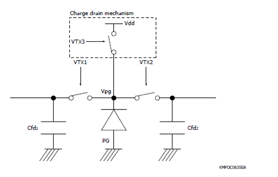
When VTX1 and VTX2 are off and VTX3 is on, the charge drain function is active and thanks to this structure it is possible to drain unneeded charges caused by background light during the non-emission period.
This structure allows us to efficiently integrate a high-speed pulse light, or pulse laser diode sources, which can be used as a shutter.
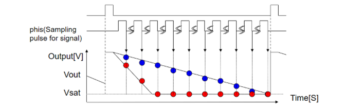
Non-destructive readout
An additional interesting feature is the non-destructive readout method that allows the output of voltages at different integration times without resetting the capacitors Cfd1 and Cfd2 in the pixel.
Figure 13: Non-destructive readout
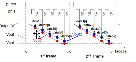
As showed in Figure 13, in each pixel of the CMOS image sensor the voltage output value during the accumulation can be read (multiple output). With this structure it is also possible to achieve low noise because the same frame difference of two data points cancels the reset noise generated when the pixel is reset. In addition, thanks to average processing, is possible to have high accuracy.
If we consider the impact of ambient light, we can have mainly two situations.
Figure 14: Non-destructive readout – advantages when applied to distance measurement system
In Figure 14, the blue points are relative to weak ambient light. In this case we do not have saturation, so all the data can be used for the calculation. The red points represent a high level of ambient light. In this case we reach saturation and the data cannot be used, however using the limited initial data, we can calculate the slope and use an appropriate integration time.
One disadvantage of non-destructive readout is that the readout is performed several times in each frame, so the frame rate decreases as the number of readouts increase.
