Germany-based photonics vendor, Jenoptik has introduced optical components and systems to help serve current trends in medical, laser, optoelectronics, semiconductor equipment, data transmission and imaging technology.
The new LS open heat sink diode laser package, for example, is specifically designed to boost the optical pumping of next-generation solid-state lasers. Compared to the standard CS package, it has the benefit of delivering higher optical output power.
Despite being similar in size to the CS, the LS has a double-side cooled open heat sink design, which enhances the laser bar's conductive cooling. As a result, it can provide superior performance compared to the CS with cw-output power levels exceeding 150 W @ 9xxnm, thus opening up opportunities in advanced pump- or direct-diode-laser (DDL) applications.
Easy upgrade of existing pump assemblies
With a form factor almost identical to the CS, Jenoptik's LS package allows for easy upgrading of existing pump assemblies, with the benefit of boosting optical (pump) power to unprecedented levels.
The company has also released a UFO Probe Card, to provide wafer manufacturers and test equipment suppliers a more efficient and productive solution to the synchronised testing of electronic and photonic components.
The Probe Card can enable the simultaneous testing of electrical and photonic functionalities at wafer level – in particular at high throughput rates in high-volume production. The optical test concept of the Probe can eliminate the need for active alignment.
The unique challenges of wafer testing
This particular solution was launched against a backdrop of some of the unique challenges presented by wafer testing. Due to the additional optical components to be tested, the test throughputs are not yet as high as for established IC functional tests, so, with advanced test solutions, overall yields can be improved,
Each UFO Probe Card is customised to the individual requirements and the respective wafer layout and is available with both cantilever and vertical needle technology. It covers the wavelength range from 1260 to 1625nm, commonly used in the telecoms and data comms sector, including polarisation maintaining for individual or all optical channels.
By incorporating the vertical needle technology, Jenoptik responded to market requirements, particularly regarding co-packaged optics and ensures the economical use of the UFO Probe in high-volume test scenarios and ATE operability.
White light source to aid surgeons
The third launch from Jenoptik is a solid-state-based colour-gamut tunable (white) light source which allows for high-brightness illumination at virtually any chromaticity setting.
Incorporating colour-gamut tuning via mixing of three or more independent colour-channels in this way can allow for imaging under different (multi-)spectral illumination conditions and therefore improve visual discrimination for the surgeon and/or future AI-based image-processing-algorithms. For minimally invasive endo-illumination such as in ophthalmic surgery, the high beam quality of the (white) light source can support gauge sizes beyond 27G.
Photonics industry advocacy in Germany
These products were officially launched at Photonics West in San Francisco, but the company has been equally busy at its global headquarters, welcoming German Vice Chancellor and Federal Minister for Economic Affairs and Climate Action, Robert Habeck to its facility as part of his tour through Saxony and Thuringia.
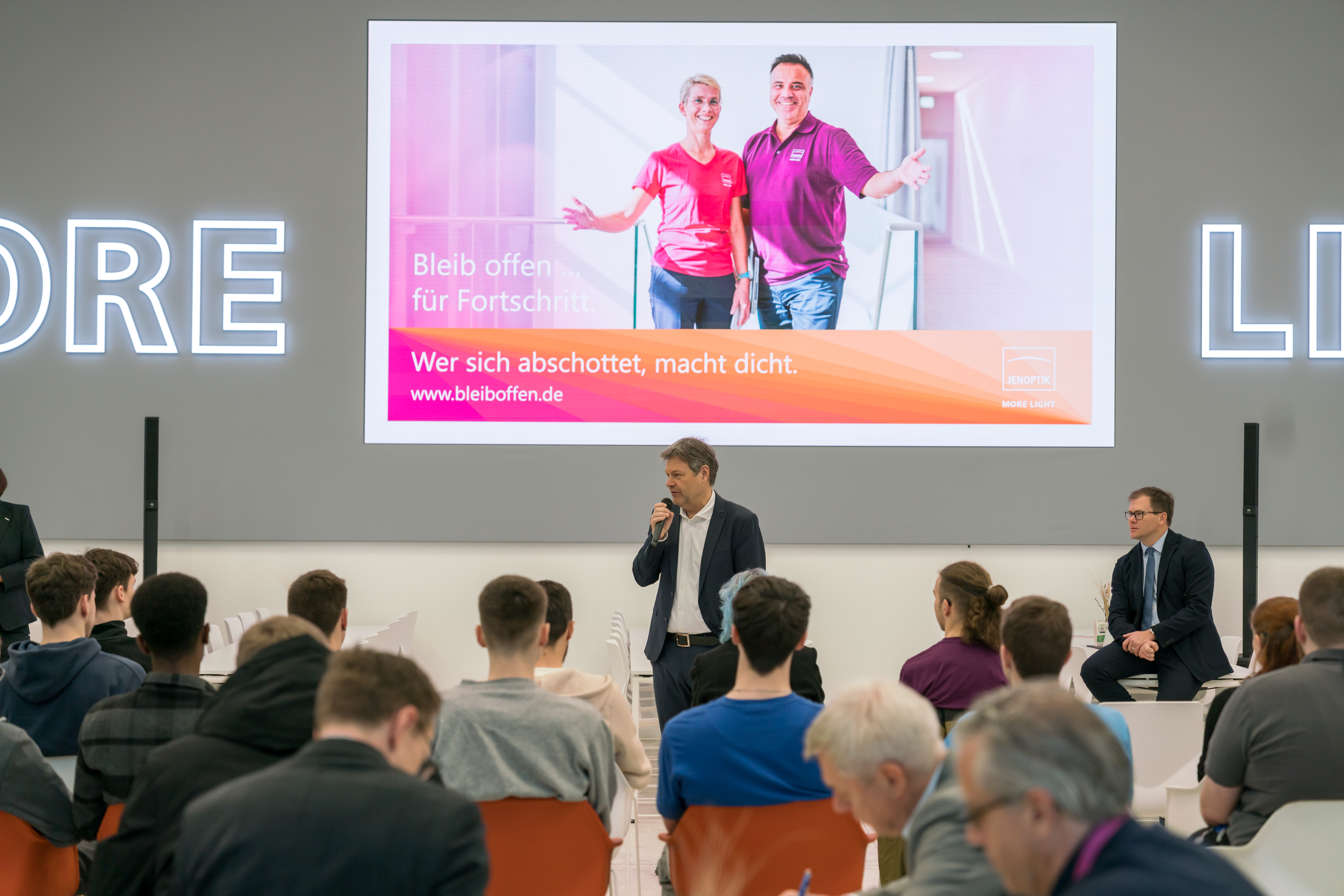
German Vice Chancellor and Federal Minister for Economic Affairs and Climate Action, Robert Habeck at the Jenopik facility
After Habek was welcomed by Jenoptik President and CEO Stefan Traeger, he took a tour of the facility, and then met with trainees and employees at the company for a discussion, in which he learned first-hand about some of challenges and experiences in the photonics industry, of everyday training and working life as well as the socio-political environment. Some of the key concerns were found to be the still differing wage levels in East and West Germany, the shortage of skilled workers and challenges in exports.