Skip to main content
Social media links EO
LinkedIn
Twitter
Log in
Register
Applications
Life sciences
Environment
Quantum
Defence
Automotive
Aerospace
Medical engineering
Electronics
Optical communication
Technologies
Illumination & energy
Imaging
Industrial lasers
Lasers & optoelectronics
Sensors, test & measurement
Photonics 100
UK Photonics
Photonics Frontiers
Resources
Webcasts
White Papers
Supplier
Events
Products
Search
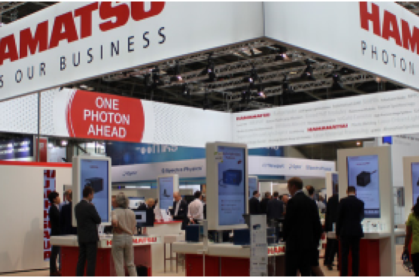
Long-standing partnership between DTU Electro and Hamamatsu Photonics results in the development of new light-detection technology
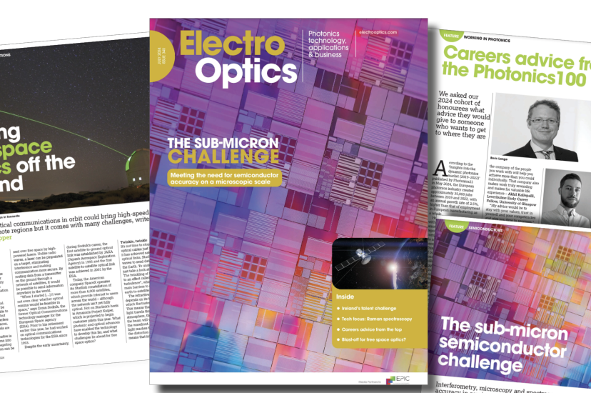
Introducing the July issue of Electro Optics
Hamamatsu completes NKT Photonics acquisition
Hamamatsu’s acquisition of NKT Photonics approved by Danish authorities
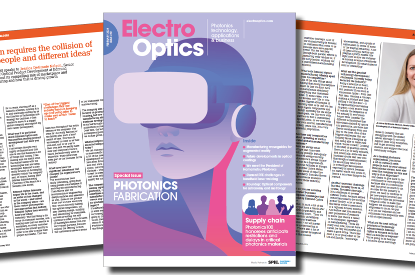
Welcome to the February edition of Electro Optics
The Photonics Leader interview: Tadashi Maruno, President, Hamamatsu Photonics
The Photonics Frontiers Award 2026 - Supporting this year’s awards
Photonics - A Key enabling technology in the quantum world
High-performance spectroscopy for field-ready LIBs systems
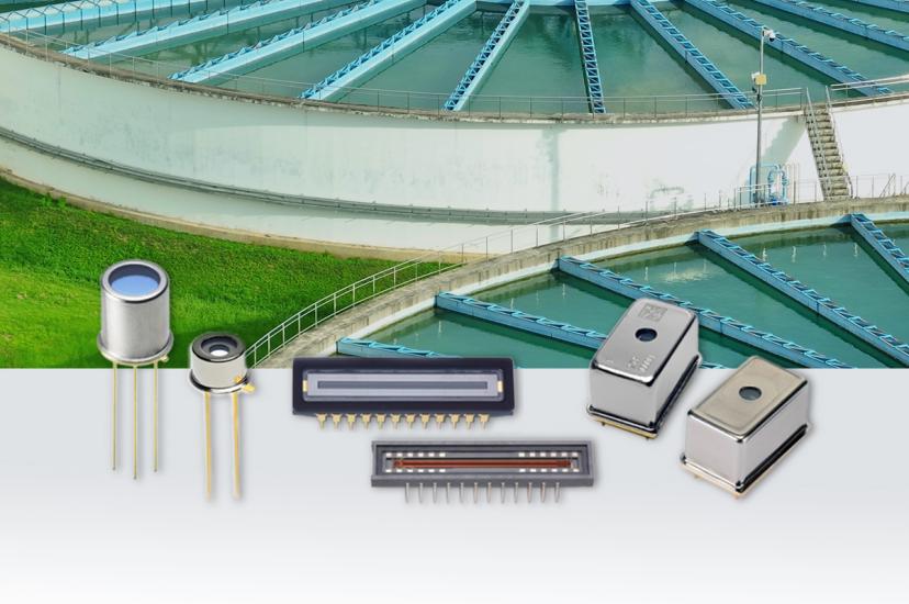
Harnessing UV-Vis spectroscopy and digital tools for smart water management
Pagination
Previous page
‹‹
Page 2
Next page
››
Media Partners


")