There is an arms race taking place in the optics sector, as laser manufacturers continually boost the output of their light sources and shorten pulse durations, while manufacturers of lenses, flats, splitters and mirrors work out how to protect their precision surfaces from the onslaught this increase in power represents.
It can be compared to an artillery battle. Gunmakers are loading more propellant into their shells, and developing armour-piercing projectiles. Tank manufacturers respond by creating stronger and more resilient armour to shrug off the incoming rounds, and the cycle continues.
The armour plating in this battle is the coatings applied to optics, and many manufacturers are working hard to keep up with the increasing demands placed on them. It’s a large and growing business, with some aspects shrouded in commercial secrecy, and some intriguing new approaches to solving the problems of laser-induced damage.
According to industry analyst Research and Markets, the global optical coating market is growing at a little over seven per cent each year and will be worth more than US$10 billion by 2020. Its report, Optical Coating Market Trends and Forecasts to 2020, published at the beginning of May 2016, records an increasing number of patents filed for optical coatings and applications by organisations around the world.
Looking at the global industry, Research and Markets projects the fastest-growing coating process to be versions of sputtering technology, particularly for filter and anti-reflective coatings in the biomedical, laser, and defence sectors. It highlights solar power as the fastest-growing end-use industry for these types of coatings, and names DuPont, Zeiss, PPG, Newport, and Nippon Sheet Glass as the dominant players in the global industry.
Damage morphology
In the more rarefied atmosphere of specialist high-power optical components, sputtering and ion assisted deposition are at the forefront of coatings developments, while electron beam systems are increasingly considered as workhorse technologies providing economical alternatives for less demanding applications.
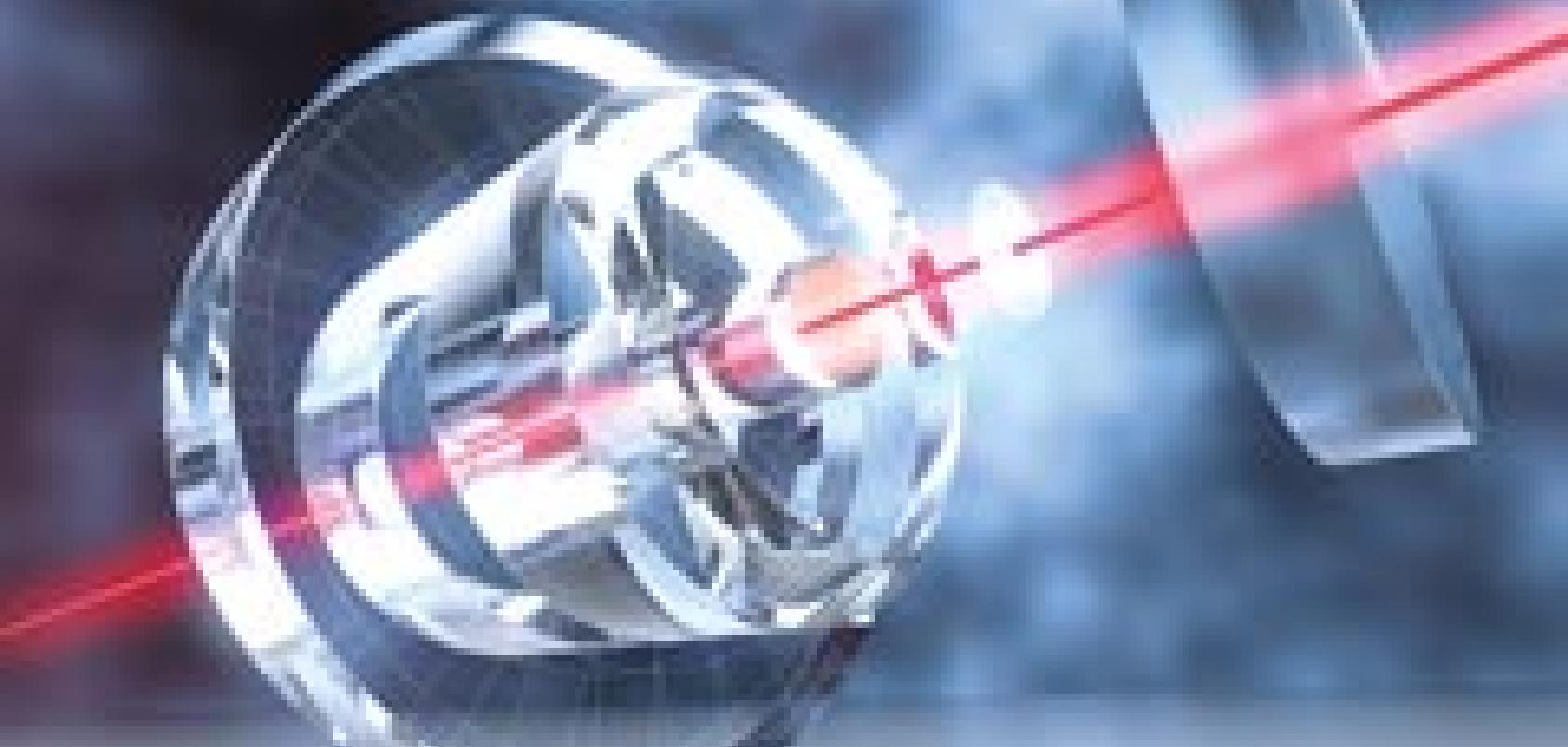
With any coating for a high-power system, the critical aspect of performance is the ability to resist damage from the light source. Generally referred to as the Laser Induced Damage Threshold (LIDT), this is a measure of the intensity of light that the optic can handle without damage to either the substrate or the coating.
When considering what constitutes a high-power optical system, Edmund Optics suggests a pragmatic approach: ‘The laser-induced damage threshold is largely dependent on the application. A reasonable definition is that a high-power optical system is one that has the potential to damage any of the coatings in use.’
This damage can manifest in a number of ways, related to the materials involved and the laser itself. Lithuania-based laser research consultancy Lidaris lists nine primary types of laser-induced damage, some of which can be diagnosed by microscopic inspection of their shape or morphology.
Pin-point damage is generally caused by the rapid heating of contaminant particles within coatings, while radial fractures and cracking may be the result of localised stress caused by multiple nanosecond or femtosecond pulses in glasses and crystals. Rather like a high-velocity bullet wound, these can exhibit different entry and exit patterns.
Femtosecond melting results in the rapid liquification and resolidifying of coating material either on the surface or within its thickness, leading to the creation of amorphous material within the coating. Metallic surfaces subject to longer pulses can be prone to surface melting and the formation of droplets.
Dielectric coatings on metal substrates can be vulnerable to delamination prompted by thermally induced stress. Components operating in high vacuum may experience outgassing of contaminants, leading to a darkening of the surface. Finally, blistering can be seen in some oxide films, caused by the relaxation of compressive stress and coupled with expansion pressure from material ablated from the substrate.
In the war to resist these multiple threats, optics manufacturers are adopting a number of innovative approaches. One thing they all agree on is that coating should not be considered in isolation from the rest of the optical component.
Helmut Kessler, managing director of Manx Precision Optics (MPO), stressed that the laser damage threshold may have less to do with the coating itself than with the quality of the substrate and the care taken in preparation. ‘If you start with a poor substrate, you can never make a good optic’, he said, comparing this to the need for good foundations on which to build a house.
MPO makes optical components for some of the world’s most powerful laser systems, used in research projects at institutions such as STFC and CERN. Kessler observed that modern ultrafast lasers exhibit a different damage pattern from ‘classical’ laser systems, and this ‘seems to indicate that there is a natural ceiling to the damage threshold you can achieve at very short pulses, governed by the electron band gap.’
If there is a physical limitation to the power that can be handled by an optical system, the industry faces two challenges. One is to get up to that ceiling, by exploiting the very best that current technology affords. The second is to find ways to get beyond the ceiling, through the development of completely new optical systems.
Close to the edge
The commercially-available technologies for high-quality optical coatings involve three main deposition methods. Different manufacturers may have slightly different names and techniques for these, but all involve depositing coating materials onto prepared substrates with the assistance of electron beams, ion beams, or sputtering – sometimes in combination.
Electron beam or e-beam coatings are the most conventional, and widely used with dielectric coating materials.
Ion assisted deposition (IAD) coatings tend to have higher damage thresholds, because during the coating process the molecules are deposited with higher energies – up to 100 electron volts compared to perhaps 0.1eV with traditional e-beam techniques, which creates more compact layers of coating material. The resulting layer is denser and purer, with lower thermal drift and a higher LIDT.
E-beam is typically the most economical process, but this does not necessarily mean it is unsuitable for high energy lasers.
Sam Thienel, technical sales engineer at Laser Components, commented: ‘The common assumption is that ion assisted deposition [IAD] or ion beam sputtering [IBS] is the best solution for a higher laser damage threshold, but this isn’t necessarily the case. We do tend to advise IBS or IAD coatings but it’s important to remember that it is not necessarily the most expensive method that gives the highest laser damage threshold for a give application.’
Illustrating the point, Thienel said that the shorter laser pulse lengths that might be assumed to be the most damaging can actually be less of a problem for cheaper e-beam coatings than the high-end IBS or IAD alternatives.
A further complication comes when the surfaces to be coated are themselves complex. Deposition Sciences introduced its line of high laser damage threshold (LDT) coatings in 2013 to provide a high damage threshold across a range of products with complex geometries. Sales and marketing director Michael Newell said that the new low insertion loss coatings offer extremely low reflectance of R< 0.25 per cent.
The coatings are aimed at a variety of critical applications on micro and fibre lenses, collimators, beam shaping optics, ball and hemispherical lenses, and even domes and reflectors. ‘Our IsoDyn low-pressure chemical vapour deposition (LPCVD) process gives us a unique capability to provide high laser damage thresholds for laser systems, with laser damage threshold levels as high as 25MW/cm2.’
Secret recipe
One thing manufacturers don’t tend to talk about so readily is the materials used to create the coatings. Dielectric metal oxides have long been favourite coating materials and have the advantage of low absorptivity. Coatings are developed and selected for specific applications, and while silicon dioxide (SiO2) may be the ‘plain vanilla’ coating of choice for low refractive index layers, much more exotic flavours are deployed for higher index layers – and these are closely guarded commercial secrets.
Coating materials include tantalum pentoxide as well as oxides of aluminium, hafnium, niobium, scandium, titanium, and zirconium. Complications may arise depending on the nature of the substrate – standard BK7 borosilicate glass, fused silica, or sapphire for instance – and the number and thickness of coating layers to be applied.
Alongside the development of new coatings recipes, manufacturers are exploring other ways to reduce laser-induced damage to optics. At Laser Components, one recent development enables laser users to spread the load by using larger optics. In spring this year, the company commissioned an IAD chamber that allows the coating of components up to 390mm diameter, compared to the previous limit of 100mm.
An alternative approach from Manx Precision Optics is to consider the optical path in a more holistic manner. With an optical flat, the flatness in operation is the critical factor. The company will sometimes polish a surface slightly concave or convex, to compensate for stresses exerted by the coating itself, or coat both sides of a component to even out those tiny stresses.
However, these effects can be overwhelmed by the simple act of mounting, which can generate wavefront errors that can ruin a high-end research experiment. To tackle this problem, MPO is collaborating with precision mount manufacturer Liop-Tek, so that packaged optical components can be delivered from a single source. Helmut Kessler is confident that the result will be what his customers really want – a better quality wavefront with high-energy lasers.
Looking to the future, it may be that today’s advanced optical manufacturing techniques are approaching the limits of what can feasibly be achieved with standard coating materials and systems. Further secret recipes will no doubt be developed, as well as cleverer ways to get the most out of optical systems, but what then?
The answer may be in some rather unconventional sounding materials, including nanorods, crystalline coatings, and aerogels.
Researchers led by Dr Garrett Cole at the University of Vienna say they have developed a crystalline coating technology that enables a tenfold reduction in mechanical losses from reflective surfaces. Using an epitaxial layer transfer technique borrowed from nanofabrication processes, they claim to have grown and bonded high-quality single-crystal films onto curved glass substrates. The work may find application in the development of narrow linewidth laser sources for use in precision measurement systems.
Meanwhile in California, researchers at the Lawrence Livermore Laboratory have created a nanocrystalline diamond aerogel that could improve the optics of low-power devices like telescopes and eyeglasses. This new form of diamond has a very low density of around 40 milligrams per cubic centimetre, only about 40 times denser than air. Lead researcher Peter Pauzauskie believes this could lead to the development of antireflection coatings more efficient than anything seen before.
It’s an area of stiff competition, with scientists at Rensselaer Polytechnic in New York having already claimed the creation of the world’s first ‘perfect’ anti-reflection coating. Fred Schubert and colleagues created a material with the lowest ever reported refractive index, at just 1.05. Using a technique called oblique angle deposition, they deposited silica nanorods at a 45° angle onto a thin film of aluminium nitride to almost eliminate reflections at all wavelengths and incoming angles of light.
These are bold claims, and none of them are yet ready for the real optical battlefield of high-energy lasers, but they might just point in the direction of the next stage of armour-plating for optics.
Due to launch in October 2018, the James Webb Space Telescope will be the most powerful ever put into space. Its 18 hexagonal mirror segments will unfold and be adjusted into shape after launch, providing more than five times the light-collecting power of the Hubble Space Telescope and promising to reveal the early universe in unprecedented detail.
The project is currently in an advanced stage of assembly, with each of the 1.32m primary mirror hexagons, plus secondaries, installed on the carrier structure. These segments are made of beryllium, chosen for its light weight, stiffness, and stability at cryogenic temperatures.
The actual reflective surface is a 120nm thick coating of gold, applied by vacuum vapour deposition to the beryllium segments by Quantum Coating in New Jersey, USA. Gold has excellent reflectivity at the infrared wavelengths at which Webb operates. The gold is in turn protected by a thin layer of amorphous SiO2 against potential handling damage.
Despite its much larger mirror, equivalent to a single 6.5m diameter primary, the Webb telescope has a mass of only about 6.5 tonnes – just half that of Hubble. The primary mirror coating, arguably the part that does the real work, accounts for just 41g of that.