Researchers have devised a new way of generating thin 3D photonic crystals that show promise for miniaturising photonic integrated circuits
Similar to how the semiconductors in computer chips manipulate electronic current, photonic crystals are nanostructures that manipulate photons.
However, while in semiconductors a periodic potential affects the flow of electrons by defining allowed and forbidden energy bands, in photonic crystals a periodic variation of refractive index – on the scale of visible light – produces a photonic band gap that affects how photons propagate.
Light in certain wavelength ranges can pass through the band gap, while light in other wavelength ranges is reflected.
Such structures can be found in nature, in the wings of tropical butterflies, for instance, that give them their iridescent colouring. Their properties make them attractive optical materials for controlling and manipulating light flow in a range of photonics applications. 1D photonic crystals can be found in the low- and high-reflective coatings on lenses and mirrors, while 2D crystals have found application in hollow core photonic crystal fibres.
It is these 2D structures that are the focus of the majority of research in the field of photonic crystals, according to Professor Willem Vos from the MESA+ Institute for Nanotechnology at the University of Twente. Now, however, thanks to his remote collaboration with researchers from the University of Tokyo, the University of Electro-Communications in Tokyo, and the Kyoto Institute of Technology, photonic crystals are being brought out of the 2D plane and into the third dimension, which the researchers say will open up a new range of applications and possibilities.
In the journal Physical Review B, Vos and his colleagues have described a type of 3D photonic crystal that they say could revolutionise the design and fabrication of optoelectronic devices for efficient telecommunication and computers, and thin solar cells.
While light can easily scatter out of a 2D crystal plane, 3D crystals can prevent light from escaping, making them interesting for applications where the light needs to be controlled very carefully. 3D photonic crystals have been explored and fabricated in the past, however they have either previously been too bulky for practical application, or have been produced using methods that cannot easily be scaled up for commercial application.
‘Our approach can be seen as a technology push to make thinner 3D photonic crystals in a more practical manner,’ said Vos. ‘The aim of our research is to see how narrow we can make these crystal structures.’
The researchers are assembling their photonic crystals layer by layer in a so-called ‘woodpile structure’, seen below.
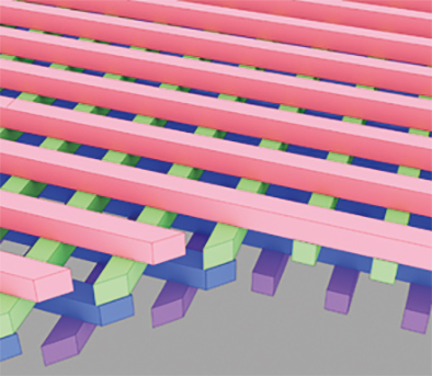
Cartoon of the woodpile photonic crystal structure that has a similar structure as a diamond crystal but a thousand times magnified. (Image: Tajiri et al.)
Dr Takeyoshi Tajiri, lead author of the paper, said: ‘Our crystals consist of stacked arrays of rods in two perpendicular directions in a semiconductor wafer such as gallium arsenide. The crystal structure is inspired by diamond gemstones.’
The advanced method conveniently allows them to make thin structures of only a few layers thick, between a few hundred nanometres to about one micron.
To investigate the new crystals, the Japanese-Dutch team decided to measure their reflectivity spectra. Therefore, after fabrication in Japan, they were shipped to Twente for microscopic measurements. The spectra showed that the thin diamond-like photonic crystals function remarkably well: all crystals showed both high reflectivity and broad peaks. Remarkably, this occurred even for the thinnest crystal.
The reflected light is forbidden to enter crystals over a considerable range of wavelengths, also known as a forbidden gap. In the researchers’ new crystals, the situation is even more radical, since the light is forbidden to travel in all directions simultaneously. ‘The quick formation of the forbidden gap in our crystals is remarkable, because earlier 3D crystals required a large thickness for a gap to emerge,’ Tajiri explained.
Smaller circuits
So where will these new crystals find application? The answer is in the miniaturisation of photonic integrated circuits.
While in an electronic computer chip, transistors can be made smaller and smaller in accordance with Moore’s Law, the optics on photonics integrated circuits are limited by the wavelength of light.
‘Given we are usually working in the telecom wavelength of 1,500nm, that sets the scale,’ said Vos. ‘The traditional way that the optics of these circuits works is on a two-dimensional plane. But these optics tend to have a large footprint due to this limitation.’
However, just as in a city a skyscraper can be used to minimise the footprint of real estate, the researchers’ new crystals could be used to guide light up and out of a two-dimensional circuit, creating three-dimensional photonic integrated circuits with a smaller 2D footprint.
This will be particularly interesting when merging electronics with photonics, according to Vos.
‘There’s previously been a misconception in industry that photonic chips will replace electronic chips. This is not the case, each offers their own advantages,’ he explained. ‘There’s currently a push towards heterogeneous integration, where electronic chips are combined with photonic chips.’
While chips such as this are already on the market from firms like IBM, from the researchers’ point of view, the photonic elements of these chips are still somewhat bulky.
‘This is where our crystals come in,’ Vos continued. ‘We believe we can make the optical layer more compact, so you can implement more optical functionality per area that can then be combined with electronics.’
While there have already been studies to realise a 3D photonic bandgap, most of the resultant crystals have been relatively large, as according to Vos it has previously been believed that in order for photonic crystals to have a suitable bandgap, they needed to be thick.
‘When I learned that Takeyoshi was able to make these crystals layer by layer, I wanted to experiment to see how the bandgap evolved in thin crystals of two, four, six and eight layers, which is the focus of our paper,’ he said. ‘This method of fabrication is more flexible, which is more amenable for integrating with circuits, the other methods are not as easy to produce large volumes with, which would make them less suited to commercialisation.’
‘Photonic crystals are seen as future components of photonic integrated circuits to be integrated into electronic integrated circuits,’ he continued. ‘We prefer the crystal parts to be small because they can be modulators. They can basically be active elements, so you can make very small non-linear elements that could serve as a switch or storage. All these functions already exist on an electronic chip. However, while they do also exist in optics, they currently have a large footprint. Since everything is about miniaturisation, it’s all about making devices smaller and smaller. This is why we are moving to photonics crystals.’
He also remarked that the fact that even thin photonic crystal structures are fully functional is great news for applications in photovoltaics, as here scientists are looking for thin broadband back reflectors to improve the performance of thin solar cells.
Both Vos and Tajiri noted how their research is a perfect example of how collaborative work can still be done remotely, despite the travel restrictions in place due to Covid-19. They were able to communicate via internet conference calls, and send the crystal samples back and forth between Japan and the Netherlands for testing.