Crystals, both natural and artificial, are used across a wide range of technologies to confine and manipulate waves such as light, sound, electrons, and spins. Such technologies span consumer electronics and sensors to fibre optics, lasers, frequency generators and spectrum analysers.
However, in order to function effectively, the internal structure of a crystal must suit the desired application precisely. This is challenging due to there being an infinite range of possibilities for such structures, considering all the conceivable building blocks and their arrangements within the crystal.
Until now, when looking to wield waves for an application, scientists and engineers have had to rely on their intuition, guesswork, and costly trial-and-error to design and achieve the right crystal structure. This is because, remarkably, it has not yet been possible to predict the confinement and behaviour of waves within crystals.
Such was the topic of recent work published in Physical Review Letters by a team of researchers from the University of Twente. They have announced their development of a robust analysis tool that finally makes it possible to describe the confinement of any kind of wave – be that quantum or classical – within a given crystal structure.
The work, titled ‘Scaling theory of wave confinement in classical and quantum periodic systems’, could dramatically optimise the way engineers design photonic integrated circuits.
Describing the significance of the findings to Electro Optics, Professor Willem Vos, of the MESA+ Institute for Nanotechnology at the University of Twente, first introduced the mechanics of wielding waves via crystals for photonics applications.
“In order to use light in the function of photonic technologies – e.g. photonic circuits – you often need to store it as a standing wave in a cavity resonator within a crystal,” he explained. “It is this wave that you can then start to modulate and tune to wield the light in different applications.
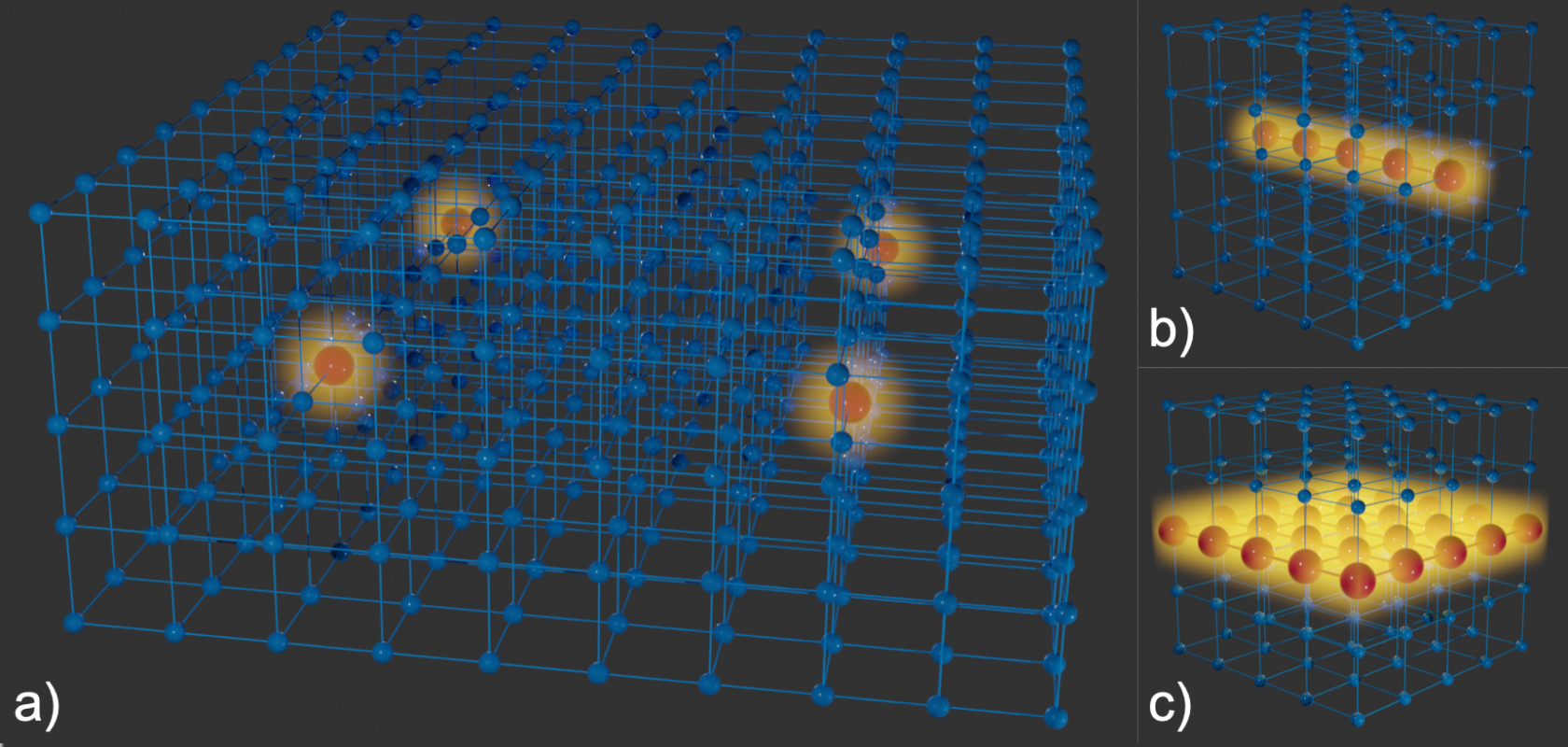
“Now, the sort of systems that we’re interested in for this particular piece of research involve confining light not just in one cavity, but in a whole array of cavities separated by sub-micron distances. These cavities aren’t just sitting in empty space, but rather within the photonic band gap of a crystal. By enabling light to jump from one cavity to the next as a wave, it is possible to create circuits, and it is in controlling this movement of light that one can start to produce very advanced photonic integrated chips.”
Regarding the extensive trial and error process that used to have to be undergone to determine the right crystal structures, Vos explained that he and his colleagues would “look naively at these cavity arrays and more or less have to estimate the way that waves would jump between the cavities.”
However, thanks to the newfound understanding described in their latest paper – the exact physical details of which go beyond the scope of Electro Optics – the researchers can now predict how light waves are shuttled around such cavity arrays within crystals.
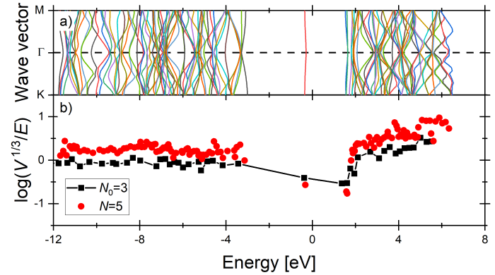
Confinement analysis of a two-dimensional quantum crystal for electrons in the semiconductor hexagonal boron-nitride with a nitrogen vacancy. (a) Dispersion relations of the crystal. (b) Ratio of the confinement volume to confinement energy computed for each propagating band of waves. (Image: Vos et al)
“We can now determine whether light waves will be transported in either: an organised waveguide-like fashion; as packets of three dimensionally confined light; or instead as a unbounded, unorganised wave,” said Vos. “The best part is that this new understanding doesn’t just apply to light waves, but also those regarding sound, electrons, quantum spins – any kind of wave really. This is why the paper includes ‘classical and quantum’ in the title, because all waves behave by the same set of rules within crystals.
As a result, this work is gathering attention across a range of communities, not just photonics, according to Vos.
He added that this research has been very eye-opening for him and his colleagues, as they initially believed the behaviour of waves within crystals would have already been defined in solid-state physics text books, “however we couldn’t find anything describing it anywhere,” Vos remarked.
New software for streamlining circuit design
Now the researchers have determined the exact ‘rules’ by which waves are confined in crystal structures, Vos and his colleagues have been able to write them into a computer program that has the potential to dramatically optimise the way in which photonic circuits are designed.
“The user simply has to input a crystal structure into our software to be told exactly how the waves will behave when moving between the cavity arrays within,” Vos explained. “For example, a photonics engineer could just input certain gizmos from their own design software, and our software would give them the required wave behaviour information.”
He added that should any photonics engineers wish to learn more about this software, they need only get in touch (w.l.vos@utwente.nl or m.kozon@utwente.nl). “We can provide them with the details of how to use the software,” said Vos. “We wouldn’t even need to know the intricate, IP-protected details of the crystal structures they’re working on, as we’d just need to tell them which gizmos to input from their own software.”
In addition to streamlining the design of photonic circuits, the new research could also add more flexibility to the process, Vos continued: “It has also revealed that there are many more ways in which light can jump in a controlled manner from cavity to cavity than we previously thought. In the past we thought there were just one or two ways, whereas now we can see there are at least twenty. This new understanding of wave behaviour could also enable the use of many more frequencies of light within photonic crystals, meaning that rather than being able to wield just one or two bandwidths, we could now use around 20 – increasing the information density dramatically. This has huge potential in terms of the capabilities of photonic circuits across a whole range of applications and technologies.”
As to what’s next for Vos and his colleagues, in the future they plan to generalise the analysis methods of the current software using machine learning, which will be the focus of their next paper. “This will really be of use to the photonics industry,” Vos noted. “Engineers will not only be able to learn more about the way light will move around their photonic crystals, but the software will also be able to provide recommendations to further optimise the design of the crystal itself.”
Linking the new work back to previous research he and his colleagues have shared with Electro Optics, Vos concluded that his ‘final dream’ is to simplify the design and creation of innovative 3D photonic circuits for the sustainable usage of high-tech devices across a wide range of industries and applications.
This research described in this article was done in the groups Complex Photonic Systems (COPS) and Mathematics of Computational Science (MACS) within University of Twente’s MESA+ Institute for Nanotechnology. The new paper, by Marek Kozoň, Ad Lagendijk, Matthias Schlottbom, Jaap van der Vegt and Willem Vos, was published in Physical Review Letters in October.
The work was supported by the Shell-NWO/FOM programme ‘Computational Sciences for Energy Research’ (CSER), by the NWO-TTW Perspectief programme P15-36 ‘Free-form scattering optics’ (FFSO, in collaboration with numerous high-tech industries), by the NWO Open Competitie ENW-GROOT ‘Self-Assembled lcosahedral Photonic Quasicrystals with a Band Gap for Visible Light’, and the MESA+ section Applied Nanophotonics (ANP).