Globally, the solar industry continues to be in dynamic growth, especially in China and Southeast Asia, with India rapidly becoming the main driver of the market. In the past few years, Isra Vision alone has installed, on average, a couple of hundred systems per year – 90 per cent of which were in Asia.
But the industry is also seeing ‘the signs of a renaissance of the solar industry in Europe’, according to Christian Probst, Managing Director Isra Vision – GP Inspect. “The war in Ukraine and the resulting political developments will accelerate growth,” he says.
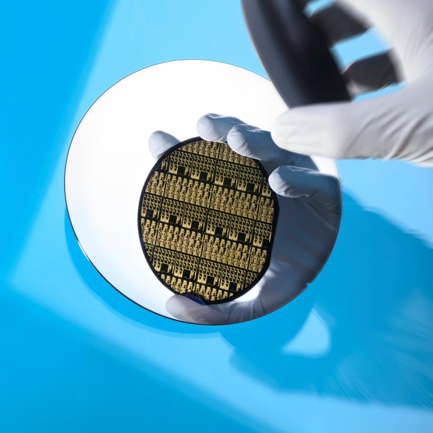
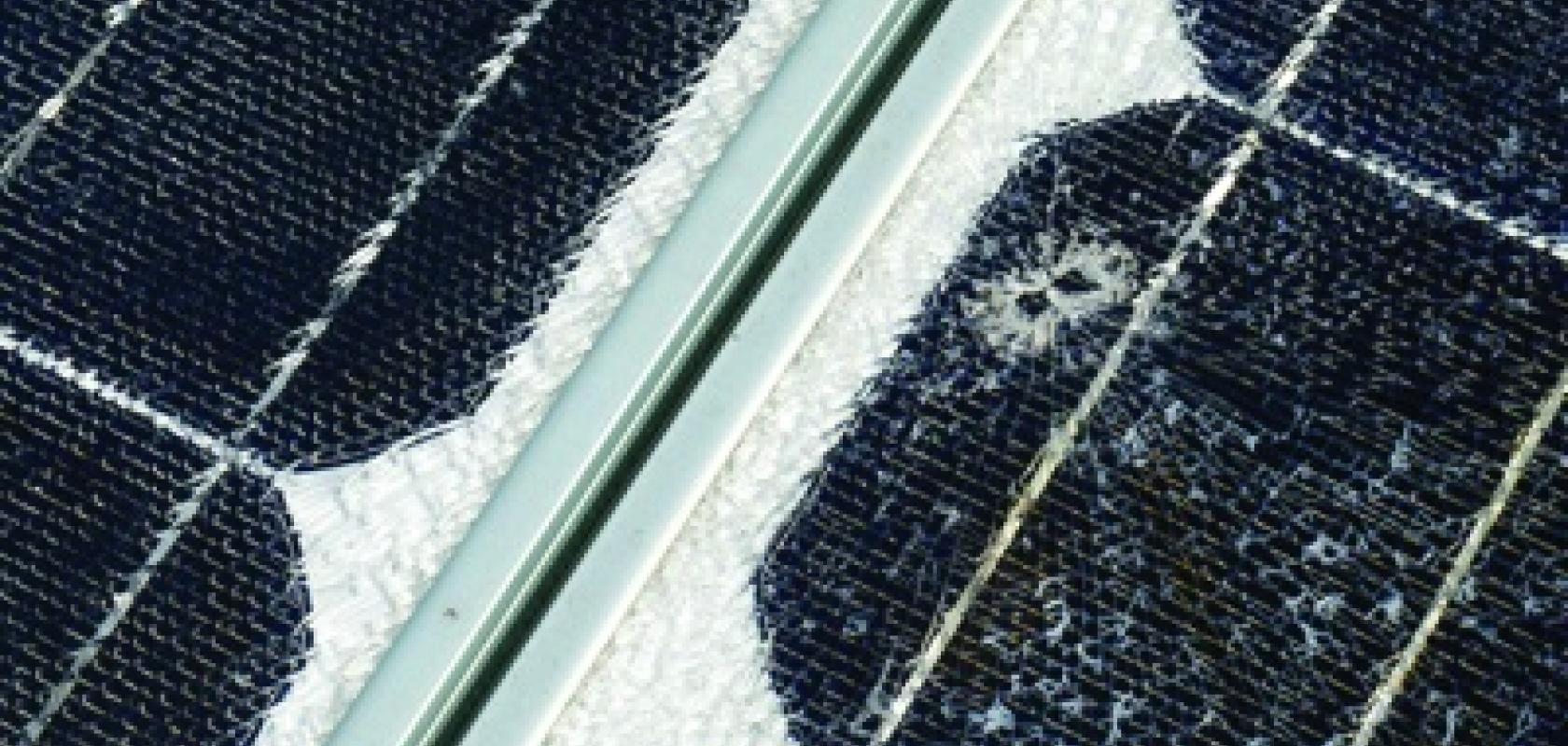
But even in the face of huge growth, the solar industry is not an area in which quality can be compromised. During production, inspection systems examine the surface conditions and geometry of the wafer, checking for distortion, cracks, chips and contamination. Microcracks can eventually cause an entire panel to shatter, causing possible knock-on damage to equipment and other panels in the array and requiring an expensive shutdown of the line for clean up and repairs.
It is therefore no surprise to hear from Xing-Fei He, Senior Product Manager at Teledyne Dalsa, that “solar cell manufacturers are moving to 100 per cent inspection of each panel after every major processing step. They are under pressure to increase the quality of their products and reduce costs. Yield is critical, and optical inspection is a vital tool”.
When is the right time to inspect solar panels?
“The inspection of solar cells can take place at various stages of the production process,” says Probst. “However, this also depends on the producer. Does it want to detect defective cells already within the process and reject them as quickly as possible? Or is a final inspection at the end of the production line sufficient?”
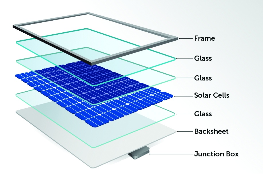 The Isra Vision – GP Inspect portfolio starts with the incoming inspection for raw wafers, where they are checked for surface defects, microcracks or chippings. This is usually followed by texture monitoring, where the quality of the surface is reviewed after the chemical bath. Next comes coating inspection, followed by print and structure inspection on the front and rear sides, and the final cell classification and sorting.
Dr Jonas Haunschild, Head of the Inline Wafer, Process Analytics and Production Control Group at the Fraunhofer Institute for Solar Energy Systems ISE, says that one of the greatest challenges lies in characterising the many interacting thin layers that make up modern solar cells. Each of these layers must be controlled, preferably not only at one point but over the entire surface.
Probst agrees the fineness of the layers and the weak contrast between them makes inspection very challenging: “Different structures within the cell must precisely align with each other to achieve the highest possible efficiency. Meanwhile, these structures are so fine that the regions responsible for charge separation are only a few hundred micrometres apart. The patterns are only faintly visible and often have shallow contrast.
“Depending on the layer, this is already very demanding, but we want to go one step further,” explains Haunschild. “The processes to be developed should be so fast and so cheap that they can be used in the production environment of solar cell manufacturers.”
Checking flexible photovoltaic panels
Back in 2018, 16 partners joined forces as part of the EU-funded OledSolar project to accelerate the widespread commercialisation of organic light-emitting diodes (OLEDs) with thin-film solar cells. Focused on developing innovative manufacturing, monitoring and inspection processes, the technologies developed during the project, which closed in 2022, may help deliver new types of solar-powered devices, such as energy-efficient lighting, flexible display screens and solar panels that could be smoothly integrated into the structure of buildings.
 TWI, based in Cambridge, UK, was one of the project partners. Working closely with the project co-ordinators, VTT Technical Research Centre of Finland, TWI has been developing inline quality-control techniques for photovoltaic module production, with the aim of automating a defect detection method for roll-to-roll printed flexible solar cells, ultimately improving quality, yield, processing efficiency and sustainability.
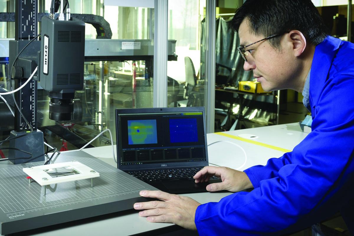
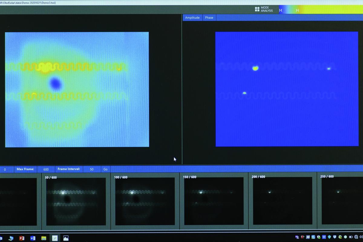
“We developed our thermography system here at TWI and that was then taken to VTT to be integrated with its production system,” explains Martin Bourton, Principal Project Leader. It made sense for the TWI team to go for an approach making use of dark lock-in thermography (DLIT). Inspected parts are usually in thermal equilibrium. When it comes to photovoltaic materials, the main options for creating a thermal contrast between defects and the background material are either applying a current light source or introducing a new one. Both approaches can spread heat through the sample and muddy spatial resolution, but it was reasoned that voltage could be more easily regulated. This also worked well for VTT’s testing line.”
TWI’s DLIT system has proved a success in the lab and in field trials, where it has been validated on VTT’s roll-to-roll pilot line. The new approach identified sub-millimetre defects (appearing as hot spots) far more clearly than standard inspection methods. “The system looked at hundreds of pieces and successfully identified all the defects that had been artificially introduced onto the sample to replicate defective printing,” confirms TWI’s Senior Project Leader, Haitao Zheng.
When the electrical characterisation of the printed film begins, it triggers the synchronised thermography inspection by an infrared thermal camera located below the test area. TWI’s DLIT system applies a square wave current to heat the test film and a thermal image is produced, ready for post-processing.
 TWI’s custom-designed relay circuit switches the power supply on and off according to the square wave generated. This enables high voltages to be applied using a low-voltage signal. As well as capturing thermal images, the camera also records the synchronised square wave reference signal created by a signal generator.
“We also developed a graphical user interface software in-house, which provides thermography data acquisition, data visualisation, lock-in post-processing and data analysis capabilities,” says Zheng. “When we compare our DLIT system to the standard approach, you can see there is far less background noise and our processed image shows defects very clearly.”
And the biggest challenge? “That has been the inline implementation,” says Zheng. “DLIT is not as fast as standard inspection methods. It’s a stop-and-go inspection approach, requiring about 20 to 30 seconds between the input signal and post-processing.”
TWI is now looking to optimise the system to develop it into a commercial product, Zheng explains. “We’re looking to improve the speed, by developing a shorter input signal and programming the post-processing software in the C programming language, rather than using Matlab and Python, for example.”
SPONSORED: Material quality is crucial in semiconductors development
Semiconductor materials are omnipresent in the electronics supply chain in various forms. Used in wafers, thin films, transistors, and diodes, in microchips and solar cells. For every development or production step, the quality of the material, as well as its optoelectronic properties, must be understood and qualified.
Silicon carbide (SiC) is a very promising material for high-temperature, high-frequency and high-power applications in electronic devices. However, the commercialisation of many SiC-based electronic devices has been challenging because of a variety of extended defects. Although conventional electroluminescence methods can help to identify the extended defects, they fall short when it comes to understanding the formation and proliferation of these extended defects. Researchers implemented a global hyperspectral electroluminescence imaging technique to help identify the luminescence band of the various classes of faults, and this will empower a better understanding of the formation of defects and their propagation in SiC materials.
There is an array of extended defects within SiC. Three of the most detrimental are threading dislocations, ingrown stacking faults, and recombination-induced stacking faults (RISFs). RISFs have been difficult to manage because they expand during device operations and lead to continuous increases in the turn-on voltage of bipolar devices, such as pin diodes. The expansion is induced through the recombination of free carriers near the RISFs. Understanding the mechanism for their motion is tantamount to their mitigation.
Electroluminescence (EL) is commonly used to identify the extended defects: RISFs emit at 2.89 eV (430 nm) and the partial dislocations (PDs) that bound the faulted regions are known to emit at 1.8 eV (690 nm). In 4H-SiC, partial dislocations also developed a green luminescence along the carbon-core partial dislocations during device operation. This emission is retained, even if the RISFs are contracted via annealing.
Hyperspectral imaging
The need to better understand the formation of defects and their propagation in SiC necessitates an interrogation method beyond conventional electroluminescence. Hyperspectral imaging, both macro-and microscopic, can provide rapid electroluminescence (EL), photoluminescence (PL), reflectance and transmittance maps. To date, it has been successfully employed to characterise different defects present in SiC pin diodes and to study the uniformity of optoelectronic properties in Perovskite, CIGS, CIS, and GaAs solar cells. By combining global imaging with hyperspectral imaging, users can analyse the optoelectronic properties in a record time. It also allows for faster identification of the composition and stoichiometry, while providing spatial distribution of stresses and strains. In other cases, spatial observation of defects, constraints and optoelectronic properties can be made using both hyperspectral macro- and microscopy to acquire rapid electroluminescence (EL) and photoluminescence (PL) maps.
Hyperspectral electroluminescence characterisation of silicon carbides defects
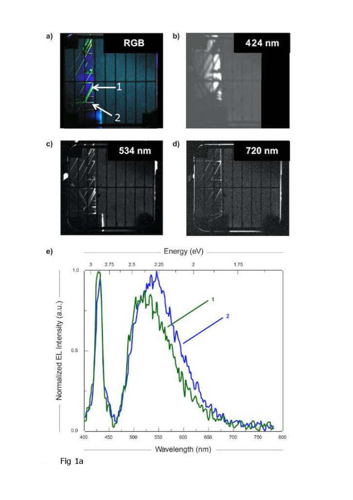
Researchers utilised IMA, Photon etc.’s (Montreal, Canada) global hyperspectral imager to acquire spectral and spatial information of the defects simultaneously. EL imaging of the SiC pin diode was performed after successive periods of device operation and subsequent annealing in a nitrogen atmosphere at 700 ºC to contract the RISFs (Fig. 1 a). Following the expansion of the RISFs, the EL from the device was collected from 400 nm to 780 nm, with a 2 nm step and an exposition time of 30 seconds. The single monochromatic images collected with IMA allowed the separation of the classes of defects. In particular it could identify the peak emission of RISFs (Fig 1.b), centred at 424 nm, and (Fig 1.c-d) the partial dislocations at 534 nm and 720 nm. The spectral response of the two regions labelled with “1” and “2” (Fig. 1 e) confirmed that the PDs show a similar sharp emission at 424 nm because of the RISFs, and a broader emission at 530-540 nm. Combining spectral and spatial information, it was possible to attribute the latter emission to mobile boron impurities. Hyperspectral imaging was paramount to identifying the luminescence band of the various classes of faults. Offering spectrally resolved images, Photon etc’s hyperspectral imaging technology improves advanced material development capacities, and it will empower a better understanding of the formation of defects and their propagation in SiC materials.
IMA, available from Photonic Solutions in UK and Ireland, is a hyperspectral microscope delivering spectral and spatial information in the VIS, NIR, and SWIR range (400 nm - 1620 nm). IMA consists of an optical microscope coupled with a source meter, probes and a hyperspectral filter based on volume Bragg gratings. This system rapidly maps photoluminescence, electroluminescence, fluorescence, reflectance, and transmittance. Based on high throughput global-imaging filters, IMA is faster and more efficient than standard point-by-point or line-scan based systems. Defects in SiC can easily be detected using electroluminescence maps obtained with Photon etc’s hyperspectral imaging system.
Further information
For more information on IMA please call Dr Elaine Blackwood at 0131 664 8122, email sales@photonicsolutions.co.uk, or visit: https://bit.ly/PhotonETC