When a space industry customer approached Stratasys Direct Manufacturing to make bespoke additively manufactured components, it fittingly pushed the ‘service bureau’ to explore new frontiers. They wanted intricate injectors and nozzles for rocket engines made from copper alloys, explained Andrew Carter, a senior process and manufacturing engineer at the firm.
The components needed passageways through them to allow coolant to flow and stop them melting at fuel combustion temperatures. The kind of 3D printing processes Stratasys Direct offers would be ideally suited – yet the company didn’t work with copper alloys at that point.
Carter and his colleagues at the Californian firm decided to develop a dedicated direct metal laser sintering additive manufacturing process based on the industry-recognised C18150 copper/chromium/zirconium alloy. This approach typically uses infrared lasers to melt small pools of metal powder, fusing it together. Patterns form, as if drawn by an invisible hand, as the laser’s energy fuses the particles, then disappear as they’re completed and masked by a fresh powder deposit. The process repeats, the layers pile up, and the three-dimensional objects gradually form.
‘The challenge with copper is that it’s very thermally conductive,’ said Carter. ‘And making things more challenging, it’s very reflective of the laser wavelength in its molten form. So the energy flux going into the powder bed is very critical. And it’s very challenging to hold a stable melt pool at industry-standard deposition rates.’
To develop the approach, Stratasys Direct used infrared laser systems made by EOS that allowed Carter and his colleagues to adjust laser power, scan speed and layer thickness. A key final criteria was whether the approach produced dense structures. ‘The real challenge was to come up with a balance between optimum density, but also an efficient process,’ Carter explained.
Initially their additive manufacturing approach sacrificed a little density, which Stratasys Direct later increased using a hot isostatic pressing thermal process.
Printing pure copper
While their efforts show that existing 3D printing technology can work with copper alloys, copper itself is a bigger challenge. Consequently, engineers are improving the available techniques to launch this material into the market, while at the same time further boosting copper alloy methods.
Among them is Thomas Stoll, who works in Joerg Franke’s team at the Institute for Factory Automation and Production Systems (FAPS) at the Friedrich-Alexander-University of Erlangen-Nuremberg, Germany. He highlighted that because copper quickly conducts heat away and reflects incoming infrared laser light, it means high-energy densities must be input to melt it. He added that even laser powers up to 1kW cannot reach 97 per cent of the density of bulk copper when fusing powder. ‘Cross sections of those specimens show regular pores that hinder the usage of the material for industrial applications,’ he said, noting that the main issue is that the laser spot size is too big. This could be due to factors such as the laser heating up the focusing lens, too great a focal length on the focusing optics, or that the diameter of the beam before focusing is too narrow. The net result is ‘laser intensity too low to create a sufficient melt pool’, Stoll explained.
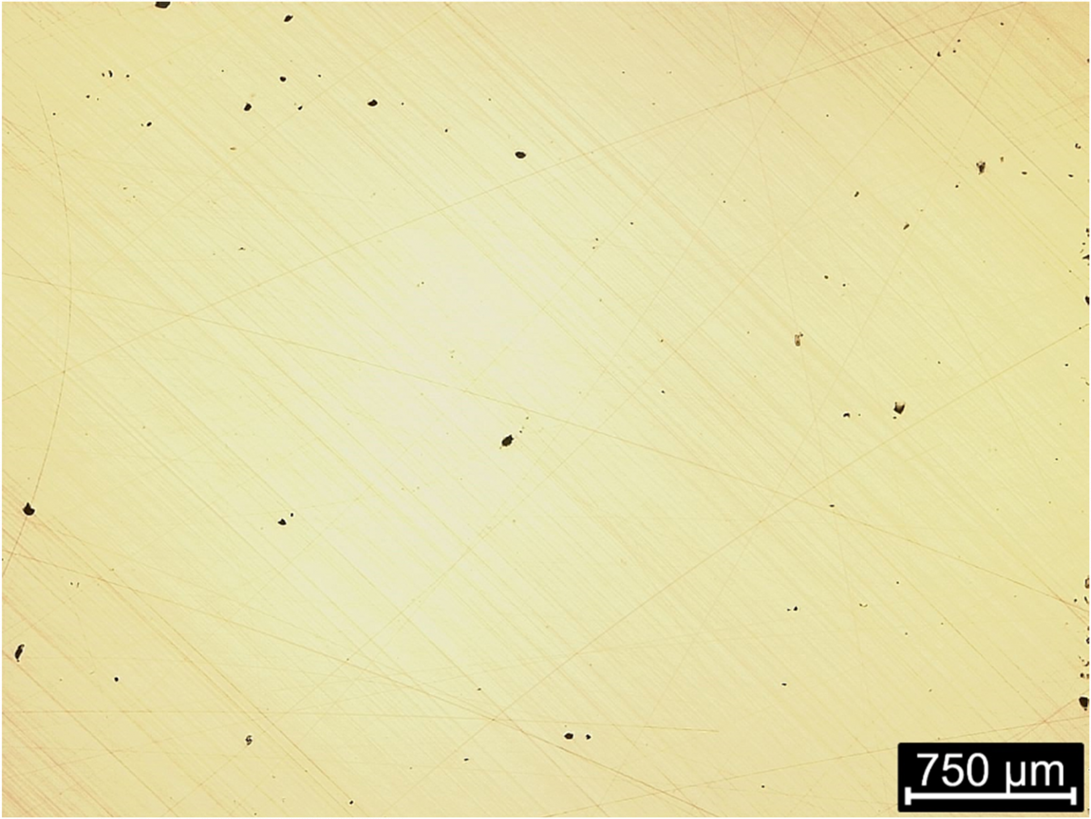
A cross-section of copper, 3d-printed using technology developed by the Institute for Factory Automation and Production Systems (FAPS), shows its high density
AI-assisted 3D printing
Stoll and his colleagues worked on this issue, considering optical process control with pyrometric cameras to control laser beam melting. ‘The thermodynamics are not totally understood,’ Stoll admitted. He has found that process factors influence the dynamics of material-light-interactions in different material states, spanning melt, solid and powder. ‘Moreover,’ he continued. ‘Different geometries need different parameter settings due to different heat distributions and vector lengths. Here, AI in combination with the mentioned process control techniques would add great value. For instance: the optical process control unit regulates the laser parameters, adapted to the heat dissipation. A widespread portfolio of different geometries and materials would give AI the chance to learn how to identify the optimal process parameters for every single layer.’
In addition to controlling the process, Stoll and his colleagues modified their infrared Concept Laser Mlab Cusing R machinery, produced by GE, to achieve minimal 25µm spot diameters. ‘The best results were reached with a spot size of 35µm at volumetric energy densities between 750 and 1,500J/mm³,’ he said. ‘The mean material density of the specimens was over 99 per cent at optimal process parameters.’
Going green
Another way of assessing 3D-printed copper is through electrical conductivity. The FAPS team was able to reach 57MS/m, close to the maximum conductivity possible in bulk copper at 57-58MS/m. Stoll notes that switching from infrared to green lasers would be ‘a perfect solution for this problem’, but that such lasers are typically very expensive. ‘As the trend goes to visible light applications due to better absorption in metals, even high-power blue lasers are being developed.’
Laser giant Trumpf has already combined its green TruDisk 1020 laser with its TruPrint 1000 additive manufacturing system. The 515nm laser is a lot closer to the wavelength where copper absorbs the most light, according to Damien Buchbinder, head of product management at Trumpf Additive Manufacturing. ‘Therefore, you really get power into the powder, and then the melt,’ he said. ‘Now you can process pure copper, which opens a wide range of new applications and mechanical properties. And the other big benefit is that copper alloys are now possible with higher productivity and better mechanical properties than before.’
Processes are two and four times faster, offsetting the slightly higher cost of adding the powerful green laser, he asserted.
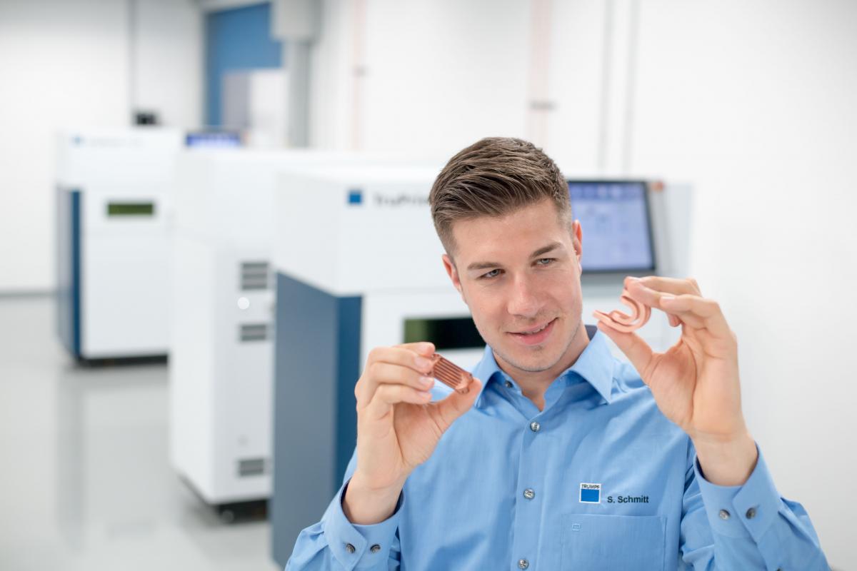
Trumpf enables copper additive manufacturing by combining its TruDisk 1020 with its TruPrint systems
The TruPrint 1000 is the company’s smallest printer, with a build volume of around 100mm3. ‘Together with the TruDisk 1020, it has a spot size of 200µm,’ Buchbinder said. ‘With it we can achieve printed wall thicknesses down to 0.4mm.’
Buchbinder also cites electrical and thermal conductivity performance according to the International Annealed Copper Standard (IACS). Several samples made by Trumpf reached 100 per cent scores according to this standard, the highest level possible.
‘This is a unique innovation point, which you don’t get right now in the laser metal fusion field with infrared wavelengths. Of course it's coming together with the high density of the material. It’s over 99.5 per cent, usually 99.8 per cent.’
In the window
The consequences of printing copper alloys like copper chrome zirconium up to four times faster than infrared wavelengths go beyond productivity gains. ‘The important thing is that our process window is bigger,’ Buchbinder said. ‘Typically, if you try to build a part but you don’t have enough energy, you have a lack of fusion, and get holes inside. If you have too much energy, you get pores, bubbles form like in cooking. Between them there’s a sweet spot. If this process window is bigger, then your process is more stable, more robust. And what we could achieve due to the green wavelengths, is a lot more of a robust process window.’
Optomec, based in New Mexico, approaches 3D printing copper from a slightly different direction. Tom Cobbs, LENS directed energy deposition (DED) product manager, said the metal’s reflectivity can affect the lasers that are melting it.
‘Laser energy reflects directly back up through the optics train and fibre cable, and back to the laser, which can damage it,’ he said. ‘Most infrared lasers will just shut down, requiring field personnel to come and reset or restart the laser.
‘Our infrared laser incorporates a built-in protection system, making it virtually immune to any back reflection, so the laser can operate at full power on reflective surfaces without any difficulty. Our testing with pure copper delivered amazing results – not only did it not shut down after extended use, but it also printed beautifully. This was not previously possible for infrared lasers.’
The resulting LDH 3.X laser deposition head can print a variety of alloys with the same light source, including highly reflective materials such as copper, with DED. ‘This allows our customers to process all metals with only one infrared laser, as opposed to needing to purchase an infrared laser for most metals and then a separate blue or green laser for reflective metals,’ Cobbs said. ‘The laser is a significant portion of the cost of a DED system, so having to purchase two different wavelength lasers in order to process two different materials is a big cost add, not to mention the added time to swap out the lasers.’
To enable this, Optomec exploits a specialised optics train in the LDH 3.X laser deposition head, which keeps the laser light collimated but changes the overall spot size at the workpiece. This enables users to employ the system over a wide range of laser powers, from 500W to 3kW. They can also optimise the process for a range of applications, from low-power thin wall builds to large heavy deposition repairs, cladding, and other applications.
‘There is considerable interest from our customers who want to use the DED process for working with reflective metals,’ Cobbs said. ‘Our new LDH 3.X laser deposition heads with variable optics are already being ordered by new and existing customers, due to the flexibility of optimising the process over a wide range of DED laser powers.’
Making the otherwise unmanufacturable
DED blows powdered material through a nozzle into a melt pool created by a laser, which brings its own challenges, potentially damaging the underlying structure. ‘If the laser spot size remains constant and the laser power increases significantly, this can cause the process to start “keyholing”, evaporating elements and basically cutting into, or through, the material,’ said Cobbs.
‘One way to avoid this is to spread the laser energy density over a larger area, enlarging the laser spot size at the workpiece. We accomplish this with the use of special optics that increase the spot size for optimal DED processing.’
Like Stratasys Direct Manufacturing, Optomec has seen interest in copper DED from the space sector. Cobbs’ colleague, marketing director Mike Dean, highlighted that Nasa has used copper liners inside Inconel alloy for a combustion chamber for liquid rocket engines.
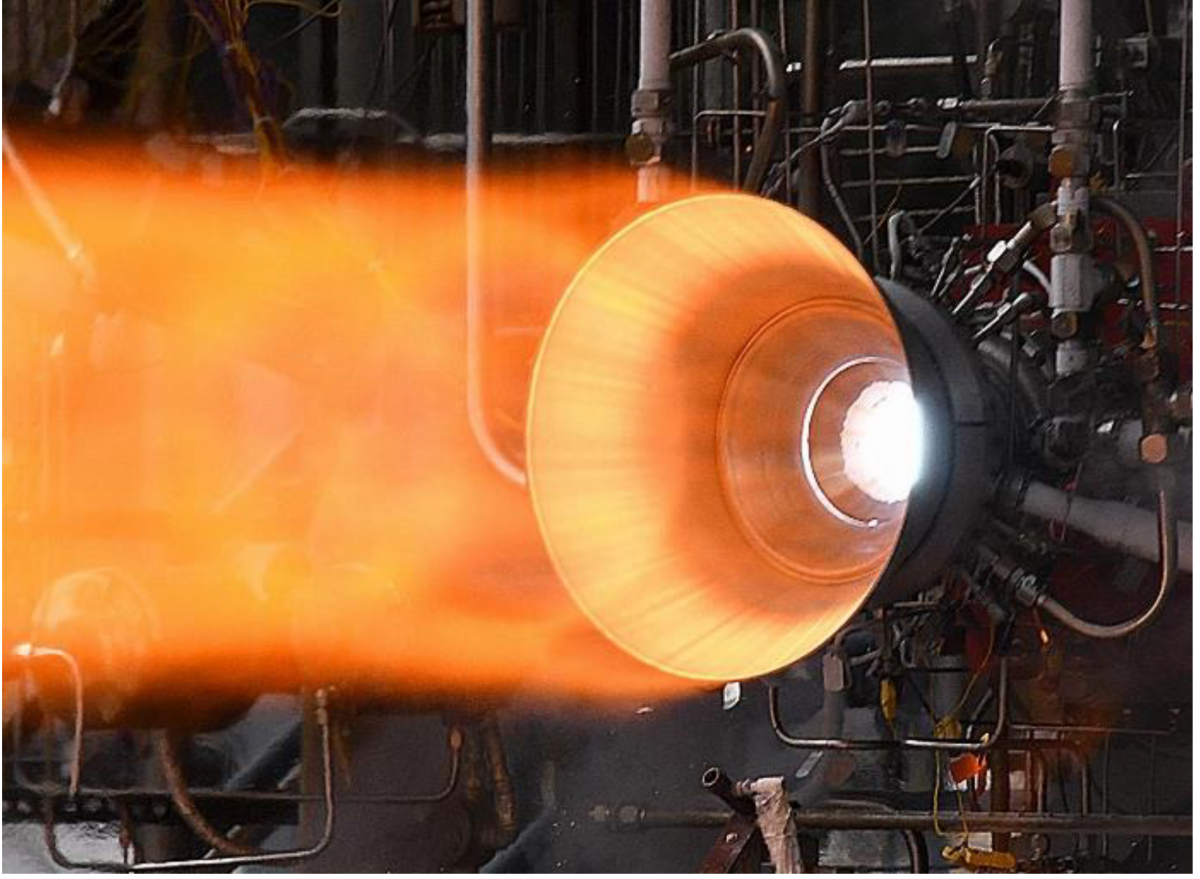
NASA produced a combustion chamber for a rocket with a copper liner made by DED additive manufacturing. Credit: NASA
Trumpf’s Buchbinder agreed. ‘Right now, there’s one market really driving the copper alloys area in additive manufacturing: the rocket area,’ he said. ‘All the burners, really big parts where they use internal cooling, they need thermal conductivity, but also mechanical resistance. That’s why they use copper alloys.’
Other important applications include producing induction coils for heating in metals such as steel, and lightweight cooling systems for electronics in electric vehicles.
Yet Carter of Stratasys Direct notes it is still early days for the technology. ‘Copper is the newest alloy we’ve brought to market,’ he said. ‘It is currently used for highly custom jobs. We hope to take it to the next level, where we start doing what Stratasys Direct calls serialised production – by no means the quantity of mass production. On the contrary, we’re talking hundreds, if not a few thousand, components. But those developments can take from 18 months to years to develop, especially with a new alloy.’
Stoll and his FAPS colleagues are looking at a different primary application to the other groups. ‘We are planning to place our research in the power electronics sector, mostly for cooling applications where 3D printing can add great value to the cooling performance. In another branch of research, we are trying to print copper directly on dielectric substrates, like ceramics for power electronic applications.’
And while 3D printing copper is still in its early stages, it’s not far behind the rest of the industry in terms of manufacturing scale. ‘When you look at the great additive manufacturing fairs like Formnext and Rapid Tech, industry is trying very hard to improve the productivity of additive manufacturing,’ Stoll said.
‘I still think additive manufacturing will settle down for small and mid-size batch production lines. The aspect of manufacturing parts that aren’t manufacturable in conventional processes, as well as product improvements with such structures, will be, and stay, the strength of additive manufacturing. But additive manufacturing technologies will find more applications in other sectors, for example electronics.’
Related links:
Stratasys Direct Manufacturing
Institute for Factory Automation and Production Systems