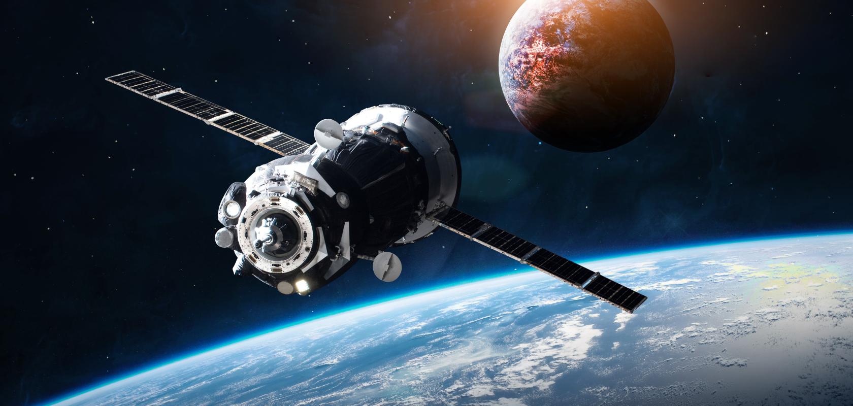
Photonics technologies for digital processing and free-space optical communications will play a key, disruptive role in the multi-billion dollar communication satellite business, it was discussed at a recent Electro Optics webinar.
The event, which covered ‘Opportunities for Photonics in the Space Sector’, highlighted how this innovation comes at a time of renewed interest in space, with the cost of access having come down considerably in recent years.
‘I refer to this as “Space Race 2.0”,’ remarked Iain Mckenzie, senior optoelectronics engineer at the European Space Agency (ESA). ‘One of the big drivers, of course, is SpaceX, which has brought innovation to the launcher market, allowing us to reduce our costs.
'But in addition to that, there's a huge amount of private capital that has been coming into the space sector, that’s pushing a lot of this innovation.’
This increased interest and investment has ramped up commercialisation within the sector, according to Mckenzie, which is now moving away from being dominated by national space agencies, as it was traditionally. ‘We're moving to a point where commercial entities are offering products and services in increasing amounts,’ he said. ‘In addition to this, there's been progress in miniaturising space loads – which further decreases the cost of launch – as well as the arrival of mega constellations such as Starlink, which are dramatically ramping up the volumes in the space market. All this has led to reduced technology development cycles and an increased appetite for risk and innovation, which has all given rise to a very interesting time characterised with fast technology development and interesting new emerging applications.’
Dealing with data processing
One of the biggest opportunities for photonics in the space sector, Mckenzie highlighted, is in data processing aboard modern satellite payloads. These are increasingly making use of digital processors to process radio frequency (RF) signals in the digital domain by taking advantage of the processing power and bandwidths offered by submicron CMOS technologies, while consuming a minimal amount of power.
‘Here photonics is providing a really important enabler because a fibre optic backplane is enabling exceptional amounts of data transfer per second through the digital optical processor, bringing with it the advantages of reduced harness mass, higher connector density, and lower power consumption,’ said Mckenzie.
The first European digital processor with an optical backplane was flown just last year in October, equipped with hundreds of transceivers and capable of achieving data processing rates of 12.5 gigabits per second. However, according to Mckenzie this is just the first of multiple generations of this technology set to be delivered to orbit in the future. ‘Prime manufacturers are already looking for solutions that push well above 56 gigabits per second,’ he said. ‘With these sorts of targets, we expect that co-packaged optics – which have been developed for data centres – will be required to realise the full potential of deep sub-micron processors in space. And so we expect this to be an interesting new direction for photonics, and one which we're supporting technology development in these areas today.’
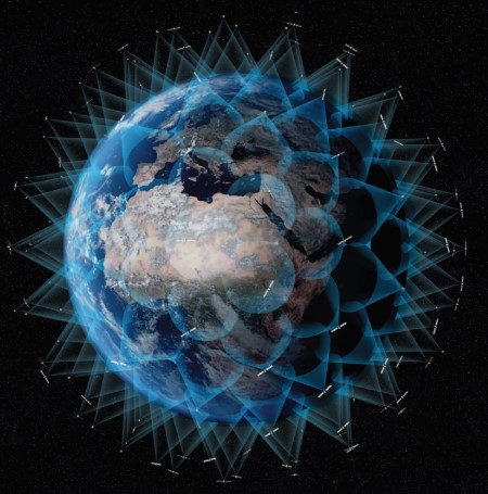
Satellite constellations are set to dramatically ramp up volume in the space sector. (Image: ESA)
In addition to processing data aboard satellites, photonics will play a key role in realising current and future satellite constellations such as Starlink, which will all be connected via free-space optical interconnects – thus providing another excellent opportunity for photonics in this sector. Here photonics can help address the limitation in bandwidth currently faced when using RF signals for satellite communications. The optical domain enables bandwidth increases of anywhere between 10 to 100 times that of RF, enabling terabits of data transfer that simply can’t be achieved in the RF domain.
‘This is one of the factors driving the push towards optical communication,’ remarked Mckenzie. ‘In addition to this you get regulatory advantages – the RF band is very strongly regulated and there is a scarcity of available RF bandwidth compared to optical domain, which is unregulated. Other advantages include optical communication being secure against jamming, interference and eavesdropping due to the optical beam having very low divergence.’
In terms of the photonics technologies involved in the terminals required for free-space optical communications, Mckenzie cited a need for highly efficient optical amplifiers, optical transceivers, adaptive optics (to cope with atmospheric turbulence), photonic lanterns, and micromirrors for optical beam steering. ‘And then if you're talking about a network of optically interconnected satellites, you also need to think about how to manage wavelength division multiplexing, possibly optical switching and routing,’ he added.
In addition to the rising application of satellite constellations, Mckenzie also noted increasing interest in using free-space optical communications for much longer link lengths, such as to the moon or beyond, to Mars, which he said will likely bring its own set of challenges.
Powering up
Peter Kean, R&D director for fibre-optic systems at Gooch & Housego (G&H), expanded on the development of optical amplifiers for intersatellite and ground-satellite free-space optical communications, citing a need for dramatic power scaling in this area.
‘We are seeing a key theme in developing optical amplifiers for free-space optical communications, particularly those with scaled up power compared to terrestrial systems,’ he confirmed. ‘This is in order to boost the signals as much as possible to overcome the extreme losses faced over the long distances involved, as well as losses experienced through the atmosphere for ground-satellite communications.’
G&H is therefore participating in programmes looking to scale up the power of optical amplifiers significantly. For example, most recently, ESA awarded the firm a contract to develop extremely powerful optical amplifiers, which G&H has dubbed project EPOS ( (Extremely Powerful Optical Sources). ‘Here the idea is to look at amplifiers for enabling terabit per second feeder links from ground to space,’ Kean explained. ‘Very high powers are required in order to overcome atmospheric loss as well as the losses just due to the sheer distance of communication. We're looking in the region of a kilowatt for ground-satellite links, and around a hundred watts for satellite-ground links, with the amplifiers supporting 25 channels of diffraction-limited light in the optical C and L bands. We’re looking to achieve this while simultaneously keeping the size, mass, and power consumption as low as possible. So that's currently a very exciting programme that we're very pleased to be working on. While the kilowatt power level is quite common in fibre lasers based at 1,060nm, it really is novel and new for 1,550nm amplifiers, and so this work is really driven by the application of this technology in space.’
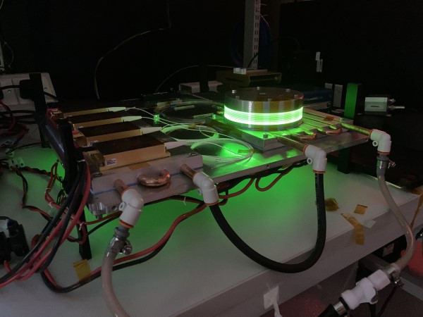
A breadboard 50W optical amplifier at 1,550nm developed by G&H. (Image: G&H)
One of the key challenges of this power scaling is looking after the thermal considerations, Kean noted, ensuring that both the pump lasers and other optical components remain cool, particularly in space where excess heat must be conducted away due to the lack of convection that comes from operating in a vacuum. Other challenges also exist in dealing with issues such as outgassing, large temperature swings that occur as the satellites move in and out of direct sunlight, and of course the ever-present radiation that the satellites must withstand once in orbit. On top of all this, the equipment must also be able to survive the mechanical challenges that come with being launched in a rocket, which itself is an extreme environment, despite only being for a short period of time.
‘G&H has, and continues to be, very much involved in supplying high-reliability fibre optic components to the subsea market, and so we're now looking at how we can translate that experience and heritage into the space sector,’ said Kean. ‘There's some key design considerations that need to be looked at, in some cases it's small tweaks, in other cases it's slightly larger design changes in order to make sure that these fused fibre optic components are suitable for the challenging environment of space. These adaptations will be vital in order to address the increasing interest and market pull we’re definitely seeing for optical transmitters, optical amplifiers and receivers and all the associated components.
Opportunities abound
Other space-based opportunities for photonics discussed in the webinar included remote sensing, global navigation, in-orbit satellite servicing and quantum key distribution.
For remote sensing applications such as Earth observation, the key photonics components include the lenses, mirrors, filters and sensor technologies required to capture and relay data back to earth.
‘For space-based imaging applications, one particular device that we've developed is an acousto-optical tunable filter (AOTF), which can be used for applications such as spectroscopic analysis,’ said Kean. ‘We've worked on several missions, both with ESA and NASA, and we’re very proud to have one of our AOTFs on the Mars perseverance rover, where it sits in the masthead analysing the emissions given off when a laser is used to vaporise rock samples.’
Laser sources have also been sent into space for lidar systems that are used, for example, to measure wind speeds and the heights of oceans, Kean continued. He also mentioned that G&H has been involved in programmes producing narrow linewidth lasers for atom cooling, in order to produce a cloud of ultra cold atoms that can then be used as an atom interferometer for sensing gravity. These systems produce incredibly sensitive measurements that can map the Earth's gravitational field.
For global navigation satellite systems (GNSS), over the last several years G&H has seen an increase in demand for fibre optic components for gyros involved in spacecraft attitude and control. ‘We’ve also seen increased demand for lasers for atomic clocks, which are used to stabilise atomic transitions that can then provide an extremely stable frequency reference even more accurate than traditional atomic clocks,’ said Kean. ‘This can help improve the positional accuracy of GNSS and give us the next step in positional accuracy for global positioning systems.’
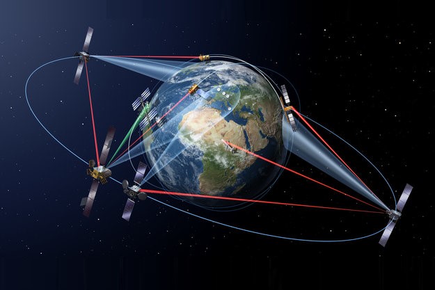
Photonics components are being used in free-space optical communications to enable faster data transfer between satellites and ground stations. (Image: ESA)
Mckenzie noted that the application of in-orbit satellite servicing could also pose an interesting opportunity for photonics going forward, where spacecraft are used to assemble, repair, add capabilities, refuel, recycle, and also remove satellites at the end of their life.
‘We've already had the first successful demonstration of this capability by Northrop Grumman with their MEV-1 and 2 Mission Extension Vehicles,’ he said. ‘MEV 1 went to a graveyard orbit, picked up a satellite that was there and brought it back into service with a five year life extension. Such an extension of life for a telecom satellite can represent millions of euros of additional value. As of today 75 satellites have already been identified as suitable candidates for life extension by the end of 2030, which represents a considerable market, and one that photonics can play an interesting role in.’
He cited another demonstration of this capability, the EU project RemoveDEBRIS, in which various space debris removal technologies were proven. ‘For this, Swiss R&D centre CSEM developed a vision-based navigation sensor using a laser head, lidar receiver and colour camera for a small satellite. The sensor enabled close proximity navigation between the satellite and debris, as well as identification of the debris' geometrical features and main tumbling axis. There are therefore opportunities for each of these photonics technologies in future instances of this application.’
Quantum key distribution could also be an opportunity ripe for seizing in the future, Mckenzie added. This could be a key element in protecting Europe's key infrastructure and communications against attack, particularly in the age when quantum computing is just around the corner. ‘The European Commission is developing a pan-european quantum communication network for the distribution of quantum keys, and ESA is responsible for the space-based component of that network – dubbed SAGA (security and cryptographic mission),’ he explained. ‘The technology required for this application has much in common with the existing optical communication terminals, with the main delta being the need for single or entangled photon laser sources, optical quantum memories and high efficiency large area single photon detectors.’
A significant source of photonics revenue?
The speakers concluded by sharing their thoughts on how significant the space sector could be in terms of being a source of photonics revenue.
‘At the moment I hesitate to give a figure but it's a relatively small portion of the overall photonics revenues, but we can see that it is growing,’ said Kean. ‘We’re seeing a lot of interest in free-space optical communications for satellite constellations, it’s incredible. This will therefore likely be a significant growth area for photonics over the next few years. The more traditional space applications photonics is involved in – such as Earth observation – will continue to develop as well.’
‘I would absolutely agree with that,’ remarked Mckenzie. This is the first time we're seeing scale applications for free-space optical communications, but also the optical interconnects for managing the data on-board the satellites within digital processors will also be a significant market for photonics.’
This article only scratches the surface of the topics covered in the recent webinar: ‘Opportunities in for Photonics in the Space Sector’, now available on demand.
SPONSORED: Scaling semiconductor manufacture for space and beyond
The journey from concept design to fullscale semiconductor manufacturing is often hindered by a number of different obstacles from diverse teams scattered across the world who simply do not understand how the manufacturing process of die bonding, wire bonding or vacuum reflow impacts the package design.
Often, start-up companies or divisions of larger companies may not have a complete team available and might not be aware of how to take their package from design to full-scale production.
It is obviously vital to get the packaging right every time and for every use case. But, particularly for applications in space, volume produced packaging must provide the same high reliability as the carefully crafted initial builds, as the fi nal assemblies may need to function in some of the harshest environments and play crucial roles where failure cannot be an option.
One of the biggest misconceptions is thinking that the process from an initial concept design to a first article build is an easy, one-step process. Producing the first build, ensuring that the packaging is indeed functional, and manufacturing it to perform exactly as expected is not always straightforward.
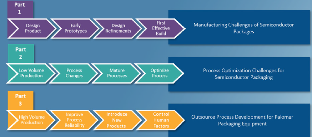
Figure 1: Three stages of manufacturing ramp-up
Step-by-step
There are several steps to follow, such as working through multiple packaging builds. Also, along the way, packaging engineers will encounter issues, which may be material-related or process-based; and the designs may need to be changed or refined one or many times in order to achieve that first effective build.
It’s very important to understand that creating a successful package requires more than one or two build quantities across all phases. Several build quantities will be necessary because a great deal of learning and discovery about the manufacturability of the package, the materials selection and the process to manufacture will happen over the production cycle. Keeping all this in mind will ensure less wasted time or extra cost. Ordering sufficient build quantities at the outset is advised to prevent waiting through multiple long procurement cycles. To mitigate those risks requires focusing on achieving a minimum viable product.
During the early prototyping phase and small volume manufacturing, there are a number of factors to focus on.
They include:
-
Tolerances: it’s important to not think of the initial design as just a prototype. Tolerances can heavily impact the ability to test the prototype.
-
Material selection: proper material selection means not only using quality materials, but also ensuring the right materials are selected.
-
Fiducials: ensuring deliberate creation of fiducials is essential to bonding at micron level.
-
Tooling and process changes: being aware of how design changes impact tooling and bonding processes can help eliminate unnecessary costs and time delays.
-
Traceability: getting to the root cause of a quality issue can be much easier if a method of traceability is used in the build process.
Take feedback on board
Once a semiconductor package has been successfully built and tested at low volume, there will likely be potential areas of improvement within the manufacturing processes. Making process changes based on feedback from early product batches will move the manufacturing towards a mature process, but can often result in some negative impact in the short term rather than positive impacts. Any time a process change is made, there will always be new elements of the process that need to be optimised or re-optimised. This typical pattern is represented in Figure 2. As there are many possible process changes and options for improving throughput or yield, ensuring the best path may be difficult, especially for new and evolving products.
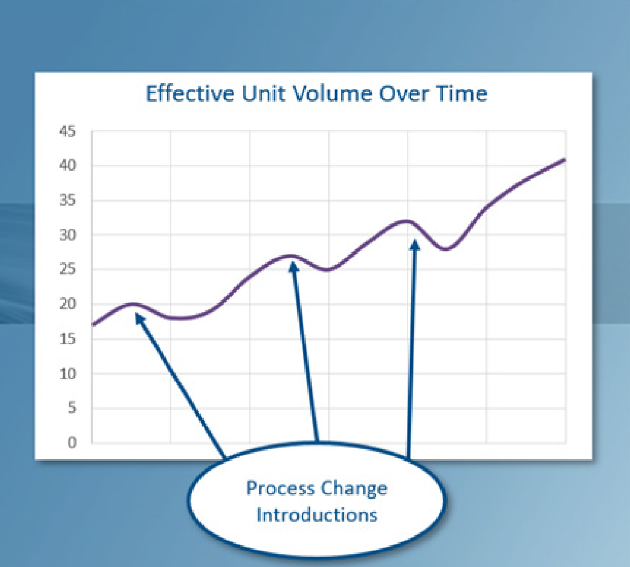
Figure 2: Simplified effects of process change
There will always be a cycle of process development where a mature version of the process will help to identify potential areas for improvement. This will, in turn, necessitate process changes that require optimisations before effective increase in production volume is seen. After the process matures again, new potential improvements will likely be found.
Lastly, as a product enters high-volume production, continuous improvements are made regardless of how robust or mature the process is. These improvements are driven by process data or from mitigating potential risks that can stem from a variety of factors. Within a stable production, it is often difficult to introduce changes into the process or develop new products or iterations. There is a constant risk of production faults occurring from peripheral influences, such as process personnel. In order to ensure optimal full-scale production of your product, it is imperative to understand the challenges present at this point in the production life cycle.
By: Kyle Schaefer and Nicholas Evans, Palomar Technologies
Further information
To learn more about the challenges faced from package design and prototyping, through process development and process optimisation, download the full article and learn how to ensure the device can indeed be manufactured with the desired throughput and quality, visit: www.electrooptics.com/ premium-access/185/ journey-full-scalesemiconductor-packagingmanufacturing