MEMS, or micro electromechanical systems, may seem like a space age technology, but it is not new; for around 20 years, scientists have been producing devices with moving mechanical parts in the scale of millimetres, micrometres, and, more recently, nanometres. However, it wasn’t until much later that scientists and engineers truly saw the capabilities these devices could possess, finding them to be cheaper, have greater integration potential and lower power consumption than the alternatives.
MEMS emerged out of the semiconductor industry, initially as an experiment in the possibility of producing such tiny mechanisms. It borrows much of the same technology, and experienced the growth and decline of the dot-com revolution, but now covers applications including astrophysics, medicine and laser communication.
The rapid growth of the telecommunications industry initially brought great demand for MEMS optical switches, a larger MEMS product at a scale of around 1mm. These tiny mirrors, moved using electrostatic forces, were used to control signals sent through optical fibres. At the time, they created a lot of excitement because they increased the efficiency and speed of the transfer of data. The optical fibres, and the switches, experienced very little loss of signal, meaning that more data flow per second was possible, and they allowed a transfer of signal without the need to translate into an electrical signal first, which is expensive and time consuming.
Unfortunately the expected demand did not meet the actual demand. The market collapsed, and with it many people’s faith in MEMS. However, it did not stall development for long. ‘There was a global realisation that an insatiable demand for high data throughput had driven the market before,’ says Susanne Arney, director of microsystems and nanotechnology at Bell Laboratories. ‘When it was discovered that this did not exist, there was a realignment between computation applications and telecommunications. That was when we learned it was better to develop a wavelength splitting switch.’
A wavelength splitting switch uses a grating to separate different wavelengths, and hence signals, in a light beam. This can also provide an even higher data workflow, at more than 1Tb per second.
Although many optical MEMS devices use tiny moveable mirrors, optical MEMS sensors use a tiny light cavity whose dimensions change according to the measurement being taken. As the dimension changes, so do the interference patterns of the light, which are measured and give the final reading. Applications include pressure sensors in cars, fuel-level sensors, microphones in cell phones and even chemical sensing
However, the major market for optical MEMS seems to be in corrective optics. One of the first optical applications was in intelligent mirrors in telescopes, now used in the Lick observatory at Santa Cruz. Light from stars forms a perfect image for millions of light years until the last hundred kilometres when it is distorted in the Earth’s atmosphere, causing the stars to appear to twinkle. In the past, telescopes were placed in orbit around Earth, above its atmosphere, to avoid these inaccuracies. However, this is expensive, and takes a lot of time to manufacture and launch into space.
To solve this problem down on Earth, Boston Micromachines developed deformable mirrors that use many actuators to pull or push the mirror surface up or down, correcting any aberrations in the image that a sensor detects. The mirrors can vary in size from 2mm (with 32 actuators) to 25mm (with up to 4000 actuators).
Moving from telescopic to microscopic applications, Boston Micromachines has been working with medical researchers to produce microscopes integrated with MEMS deformable mirrors that are currently going into clinical applications for the treatment of blindness. The small size and low cost of MEMS mirrors, due to mass production methods such as silicon wafering, have made this possible.
Many of the main causes of blindness involve macular degeneration. To treat this, doctors need to view blood vessels at scales of around 5µm, but the lens and vitreous humour distort the image of the retina, allowing images at scales of only 10-15µm. MEMS deformable mirrors, however, can give images at a resolution of just 2µm, allowing the doctor to see much more detail and make a better diagnosis.
You may expect devices with such tiny mechanisms to be very fragile, but this is not the case according to Paul Bierden, CEO and president of Boston Micromachines. ‘There are many problems when creating devices at such a small scale. People tend to forget to take special care over packaging, but once the devices are buttoned up, they are very robust and can run for tens of billions of cycles.’
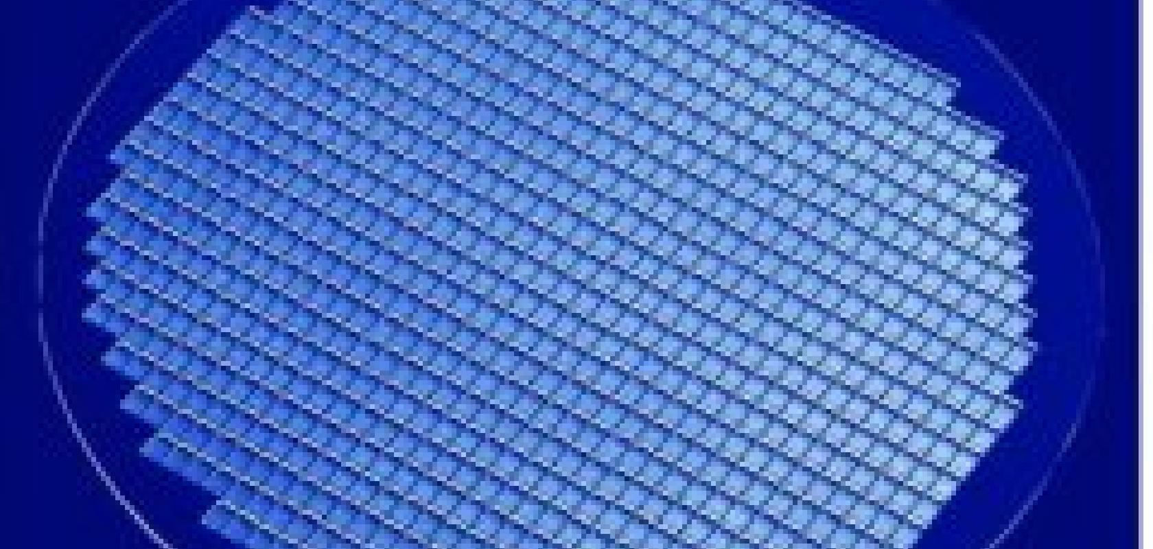
MEMS packaging protects the delicate, miniscule components from environmental effects, such as moisture and dust. The methods used have improved hugely over the past two years. MEMS devices are typically mass-produced on a silicon wafer. In the past, manufacturers would dice the wafer, and package each component separately. This was obviously a bumpy process that damaged the devices. Now, companies encapsulate the devices on the wafer, reducing the wear and tear.
In addition, Berliner Glass now uses a moulding, rather than machining, technique, to produce the housing (pictured above). This allows a greater complexity in the design, more exact replication, and reduces damage to the surface that could result in retained moisture and loosened particles that would damage the system.
Texas Instruments also produces MEMS products for medical applications, although its DMD (digital micromirror device) chip was originally designed for military, publishing and entertainment applications.
The chip is made of many tiny mirrors, which are either tilted, in which case they reflect light and give a white pixel, or flat, where they return a black pixel. It works in much the same way as when spectators in a sports stadium hold up cards to produce a larger image. The mirrors are electrostatically charged, and are about 10-12µm wide with a 13° tilt. They are toggled many times a second, and the ratio of on-time to off-time determines the shade of grey produced. Colour is produced using colour wheels, LEDs, or 3-Chip technology, in which one chip is used for each primary colour. The reflected light from all three chips is then merged to produce the correct colour image.
Originally, the chip was used for projectors in offices, churches, the classroom and home cinema, but recently engineers have found many more original applications. Cheraina Dunn, business development manager of new applications at Texas Instruments, says: ‘The biggest consumer space is in lithography. Customers use DMD in printed circuit board manufacturing, print-to-plate applications, and screen-printing. All are able to perform maskless lithography, which gives a huge cost-saving.’
It is the medical applications of the DMD chip that have produced the most exciting and wide-ranging results. Researchers are looking into building chips for gene expression. The chip would reflect light on the relevant parts of microstructures, curing the polymers. One company has even developed a scanner that can project the veins of a patient on top of their skin, facilitating the location of deep, collapsed and varicose veins. It can be also used for early diagnosis of skin/cellular abnormalities, eliminating the need for biopsies. In addition, the structure of one’s veins is unique, so it may be used for identification purposes in the future.
3D imaging is another exciting development that uses DMD chips. Again, this could have applications in entertainment, and in medicine. ‘3D images give a lot more data that could be useful for the medical profession,’ says Dunn. ‘It could be used to piece together x-ray data, in breast cancer cases, and advise the surgeons to cut from a different angle than they otherwise would have. Once the professional markets such as oil and gas and medical profession accept [this technology], then prices will drop and it will be more available for the consumer market too.’
The market seems to have changed since MEMS was first developed. Dunn believes that medicine will soon be the biggest market, ‘although clinical trials tend to slow down the availability’. Paul Bierden agrees: ‘Biological applications are experiencing the fastest growth, but across the field it is making a more solid resurgence. The usefulness is becoming apparent in many applications. MEMS has moved from being a cool technology to a useful technology. People used to buy it just to play with the latest technology, but now there are things that just can’t be done without MEMS.’
MEMS-based device to analyse lunar water content
Polychromix is collaborating with Nasa to provide digital transform spectrometers for determining water content on the surface of the moon.
Under the agreement, Nasa will outfit the Lunar Crater Observation and Sensing Satellite (LCROSS) with Polychromix near-infrared spectrometers. Nasa chose Polychromix’s technology because of its low power consumption, small size, low weight and reliability – all essential features for mission-critical applications. The Polychromix near-infrared spectrometer will be included in the research vehicle to identify the presence of water ice at the Moon’s south pole. The mission will consist of dropping a payload onto the moon’s south pole to produce a material cloud that can be analysed.
The existence of lunar ice is a hotly discussed debate. If it exists, astronauts could drink it and use it for rocket fuel. The LCROSS mission will help settle researchers’ ongoing conflicting conclusions and perhaps pave the way for humans' return to the moon.
‘We are honoured that Nasa selected Polychromix’s DTS technology for this exciting endeavour’, said Dan Klevisha, vice president of infrared systems at Polychromix. ‘Our selection for the mission is a testimonial to the breakthrough technology provided by DTS and our commitment to building quality products.'
Nanowires

NIST's nanowires
Researchers at the National Institute of Standards and Technology (NIST) have grown semiconductor wires just 12µm long that could be used in applications such as lasers and LEDs, or nanoscale tweezers used to manipulate particles in MEMS devices. They could also be used as electrical or biological sensors, by observing the effect of absorption of chemicals on their resonance.
The wires are made of gallium nitride alloys, and when excited by a laser or electric current they emit an intense glow in the UV or visible spectrum. They have been shown to emit enough light to enable reliable room-temperature measurements of their important characteristics. They are believed to have few defects, strains or impurities, resulting in a much higher light output than the bulk material.

It would be false to assume that MEMS technology is limited to the manipulation of light. VTI has developed 3D MEMS accelerometers and gyrometers that are used in the automotive industry, GPS and even mobile phones. As the MEMS component is accelerated, its capacitance changes. An electric sensor reads this and gives the acceleration. They have the advantage that the reading does not depend on an external reference point (i.e. the surface of the road), so the accuracy would not be diminished by slippage.
These sensors are now being developed to measure pressure, vibrations and angular rotation. Heikki Kuisma, vice president of technology at VTI, says: ‘The market for MEMS has been very automotive-dominated, but now they are gradually being transferred to consumer devices. If you drop a device, then by detecting the free fall you have a chance to protect the hard disk.’ These devices have also been developed for optical applications by Analog Devices; they are used to guide overhead cameras, and to guide a weapon’s laser line-of-sight.
It’s not just the application of these devices that concerns optics; because they are so small, these devices need special techniques in the design and quality control procedures. MEMS Solutions, produced by Fogale Nanotech and distributed by Armstrong Optical, is used in conjunction with stroboscopic illumination to find the dynamic characteristics of MEMS products under a variety of conditionsm, which are then compared to those predicted by finite element analysis. With a resolution of less than 0.1nm, it is ideal for MEMS scales.