For more than 2,000 years, optical modelling and design has been based on versions of ray tracing. However, such techniques have limitations when designing components containing micro- and nanostructures.
Cameras in smartphones, laptops or tablets are now very small, meaning the entire system – optoelectronics, electronics and optics – has to be shrunk to as small a size as possible. This requires an adjusted focal length and as few optical components as possible.
Optical components can be reduced in size in several ways. The oldest method is to fold the beam path – this is how a telescope becomes binoculars. Another way is to make single-aperture systems into multi-aperture systems, as demonstrated by insect eyes, which consist of hundreds to tens of thousands of very small lenses. Each micro-lens focuses light on its receptor and each optical channel produces only one pixel; the sum of the signals from each channel provides the complete image. The insect can collect enough light to form an image without overloading the brain to make sense of the information.
Micro-optics make the optical system smaller, but these lenses are also becoming flatter – inspired, in part, by origami. In this concept, the light beam propagates within a sheet of optical fibre material in a zigzag path between optical elements on the bottom and top surfaces, providing very high-performance flat optics. Another way of making large heavy optics more compact is the Fresnel principle, which allows the transition to plan optics.
‘Optics design is generally a highly complex process, no matter which software is used. As a rule, optical designers today even use several software packages to verify their results,’ noted Petra Wyrowski, marketing director at optical software firm LightTrans. The advantages of optical software are that design flaws can be corrected early in the process and thousands of ideas can be virtually tested before the first physical prototype is built. Because, for example, a camera consists of a light sensor, a lens system made of several lenses, and lighting components, design optimisation is very complicated. The simulation gives the designer unrestricted access to all components of the system, and it means development cycles and costs are minimised.
‘The optical design process includes many different steps, such as, among others, the numerical simulation of the optical system, the analysis of feasibility, tolerance calculation, scattered light sensitivity, and integration of optic mechanics and optoelectronics. Additionally, manufacturing and testing technologies must be taken into account,’ Wyrowski added.
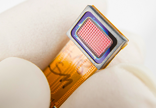
Insect-inspired micro-optics from the Fraunhofer Institute for Optics and Precision Engineering
Ray tracing algorithms are used to simulate the path of the beam through optics. However, ‘exotic optically active elements, such as a Fresnel lens or holograms, can only be modelled to a limited extent with ray tracers,’ noted Dr Peter Schreiber, a scientist at the Fraunhofer Institute for Optics and Precision Engineering (IOF).
Ray tracers can specify how big the image angle or the image area should be, along with tolerances for the production of optical systems. But more is required from these algorithms. One challenge when dealing with small systems is packaging the components. ‘When you have a small handset, there is not much room; the optical paths are often folded and you have to be very careful where optical elements and apertures are placed to avoid crosstalk or stray light,’ explained Richard Pfisterer, president of Photon Engineering.
‘The actual properties of the laser beam are usually calculated using an analytical Gaussian beam propagation tool. This tool is available in different forms in most ray tracers,’ added Schreiber. In challenging situations, for example when clipping the beam through apertures, true free-space wave propagation can be used, which now also belongs to many ray tracing software packages.
But the smaller the optical element, the more the physical properties of light will make ray tracing difficult. Diffraction effects impact on the simulation at dimensions of around 10μm, as here light travels in ways that cannot be calculated by direct ray tracing. The problem is solved with the free-space wave propagation algorithm. With even smaller system dimensions, finite-difference time-domain (FDTD) methods come into play.
Chris Normanshire, engineering service manager for Europe at Zemax, said: ‘Ray tracing is valid down to a scale of around ten times the wavelength.’ Zemax’s OpticStudio is a widely used software tool to design optical systems.
‘For smaller objects, Zemax and Lumerical have jointly developed interoperable tools that allow engineers to simulate nano-optical effects using ray tracing and Maxwell equations,’ Normanshire continued. ‘Thus, with a combination of Lumerical FDTD solutions and Zemax’s OpticStudio, ultra-thin optical component meta-surfaces can be designed.’
Schreiber commented: ‘The fact is, [optical system design] is not [possible] without ray tracing. Even if you work with wave optics, you have to eventually get back to ray tracing to build the system.’
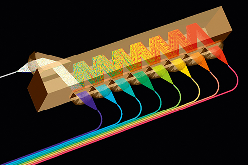
Simulation of wavelength division multiplexing
One trend is to make data exchange between CAD and ray tracers easier. ‘We feel it is better to eliminate intermediate formats, such as STEP, and allow import of the full optical model directly into mechanical CAD packages, such as SolidWorks and Creo. This is an important step in our virtual prototyping process, and is what [Zemax] software LensMechanix was designed to accomplish,’ said Normanshire.
Interference and coherence are phenomena that are typically not included in conventional ray tracing algorithms. Calculation time for fast physical optics modelling, provided in LightTrans VirtualLab Fusion, is often as fast as ray tracing and solves this problem without needing more computation time. This can also be applied to gradient optics and crystals, important for small components. Such software applications also include the use of quantum dots in display technology.
VirtualLab Fusion supports the export of optical components specified in the system into various CAD formats. ‘Using VirtualLab Fusion you start the simulation … [with] ray tracing system analysis. For more accurate calculations the software combines different Maxwell solvers in one software package with an automatic modelling technique selection,’ said Wyrowski.
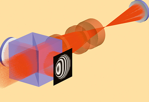
Simulation of optics for illumination
In general, not only do components become smaller when miniaturising optical systems, microstructures also usually have to have multiple functions on fewer surfaces. It is now possible to produce optics on silicon chips with dimensions down to nanometre sizes. Here, new phenomena occur, such as those found in meta-materials, an artificial structure whose permeability to electric and magnetic fields is different from standard materials. The structural features on meta-materials must be significantly smaller than the wavelength of radiation.
Here, FDTD software tools become important, offered in packages like Lumerical, RSoft, and Optiwave. ‘FDTD software is not based on ray tracing, but on confined field propagation algorithms that solve Maxwell’s equations,’ Pfisterer said. ‘[Photon Engineering’s] FRED has the ability to interface to this software by writing output files that contain the vector optical field data. The FDTD software can read these data, perform the required analyses, and then write out a vector field file that FRED can read. FRED will ultimately turn this information back into an ensemble of rays.’
Optical engineering software, such as FRED, ASAP, LightTools and TracePro, can decide which trajectories rays passing through a structure make optical sense, called non-sequential ray tracing. Another feature in optical engineering software is ray splitting. This is where a single ray hitting a surface can be split into two or more rays, each travelling in different directions. In the case of a scattering surface, a single incident ray can generate tens, hundreds or even thousands of rays. A combination of non-sequential ray tracing and ray splitting gives the software the ability to model several optical paths within a single assembly.
‘[Shrinking] optical systems is likely to continue in the near future thanks to the combination of diffractive elements and computer-aided optics,’ said Michael Berens, a scientist at the Chair for Technology of Optical Systems at RWTH Aachen University. ‘A measurement or image will only be created after processing data. Orthodox methods, such as classical geometric ray tracing, are generally not suitable for this, and one has to rely on robust numerical solutions of Maxwell’s equations, such as FDTD does, or rely on skilful approximations, such as field tracing. That takes up a lot of storage space and is still relatively slow but very accurate.'