Since 2020, anyone wanting to buy a car, or a computer, has had to wait longer for their orders, which is inconvenient for consumers, but more importantly means lost sales for manufacturers. The impact has spread across to include networking equipment and medical devices, and even chip making systems themselves, slowing efforts to recover from the shortages. Apple even forecasts that problems will continue to 2023. That’s enough of a crisis to have firmly grabbed political attention in Europe and the US.
The pandemic accelerated the digital transition, according to Werner Steinhögl, head of sector for the microelectronics and photonics industry within the European Union Directorate General for Communications Networks, Content and Technology (DG Connect). That means many more people need computers, Steinhögl told a webinar run by SPIE, the international society for optics and photonics on 21 April. ‘In the EU, there was really a supply problem,’ he said.
Steinhögl explained that building a new semiconductor fab can cost more than €10bn. Yet even if the EU provided funding to build those fabs, there is no longer sufficient expertise to manufacture chips at modern lithographic nodes smaller than 20nm, he added.
That’s significant, because lithography is the key processing step in chip making, explained Osama Awadelkarim, director of the Center for Nanotechnology Education and Utilization (CNEU) at Pennsylvania State University in the US. ‘It determines achievable device miniaturisation, and the chip making cost, since lithography constitutes most of the total cost of integrated circuit manufacturing,’ Awadelkarim said. He also noted that higher labour costs make any fabs in the US and Europe more expensive to run than those in Asia.
That would normally prevent investment, but the current chip shortages are not normal. ‘The support of the government is necessary to incentivise the chip making industry to build new fabs,’ Awadelkarim explained. ‘The other option for not building new fabs is to become dependent on chip supply from Asia. This is a very high-risk undertaking.’
Consequently, the EU and US are putting funding and support structures in place to expand local semiconductor industries. In February 2022, the European Commission announced the European Chips Act. It seeks to ‘mobilise more than €43bn of public and private investments’ to ‘ensure the EU’s security of supply, resilience and technological leadership in semiconductor technologies and applications’. It wants to increase the region’s semiconductor manufacturing market share to 20 per cent by 2030, up from around 8 per cent at present.
In the same month in the US, which has a similar share of the semiconductor market to Europe, the House of Representatives passed similar Chips for America Act investments. These totalled $52bn to strengthen domestic semiconductor manufacturing and research. Also, in the US in June 2021, senators introduced the Fabs Act to offer a 25 per cent tax credit on investments to build or improve semiconductor fabrication plants, or fabs. Lithography will be a central consideration in these acts, while photonic technologies in general may benefit.
Funding and skills
It inevitably takes time between announcing such acts and their full enactment, if they are even enacted. The Chips for America Act first appeared in the House of Representatives in June 2020. When the Senate passed it in June 2021, the Act included $39bn in grants for fab construction over five years, with officials suggesting that seven to 10 facilities might be built. The Chips for America Act also included $11.2bn for research and development, including a National Semiconductor Technology Centre, a National Packaging Centre and a national network for microelectronics research. While the February House approval seems to clear a path for the Chips for America Act to become reality, the Fabs Act has stalled in the Senate Finance Committee.
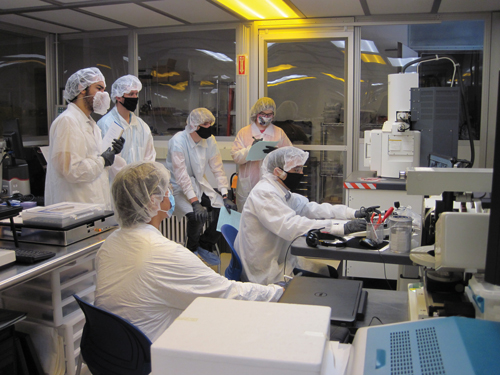
The Center for Nanotechnology Education and Utilization (CNEU) at Penn State is a model for how to boost lithography-related skills. Credit: Penn State
Beyond this, the Chips for America Act does not elaborate on the support for different areas of chip making and semiconductor processing, Awadelkarim said. ‘However, given the importance of lithography it will get the most attention,’ he added. Extreme ultraviolet (EUV) lithography for the smallest technology nodes will receive a significant portion of the funding to support research and tool enhancement and production, Awadelkarim forecasted. Another key area will be funding student training and education, and engaging industry in providing more internships and hiring of students, he added. That’s a key area of interest for Awadelkarim, who leads the pioneering CNEU at Penn State.
‘We offer microelectronics and nanomanufacturing training for students across all education levels,’ Awadelkarim explained. Six of its courses are taught at the undergraduate level as a ‘capstone semester’ in universities and community colleges, providing a qualification in nanotechnology or nanomanufacturing. ‘Over the past 20 years, close to a thousand students have attended the capstone semester and most of them are now working for nanomanufacturing companies, mostly semiconductor companies,’ Awadelkarim said. ‘Lithography training and education is given a large space in these courses.’
In February 2022, Awadelkarim testified to the US House Subcommittee on Research and Technology, in its ‘Strengthening the US Microelectronics Workforce’ hearing. He presented the CNEU model as one way to prepare the workforce for the needs of the Chips for America Act. But he also urged speedy action on authorising funding. ‘Congress has been moving very slowly,’ Awadelkarim commented. He noted that the semiconductor industry, politicians and academia are all urging that full funding be granted for both the Chips for America and Fabs Acts. ‘I am hopeful that the bill would be signed by the President before the end of this year,’ he said.
Photonics included
Meanwhile, the European Chips Act proposes actions that rest on three pillars, Steinhögl explained. Pillar one is the Chips for Europe Initiative, which is focused on research, including synergies with existing EU research programmes; infrastructure building; and supporting start-ups and small-to-medium-sized entities (SMEs). Pillar two is called Security of Supply, creating incentives for investors to build fabs to increase production capacity. Pillar three involves monitoring supply chains to anticipate and respond to potential future shortages. ‘We started in negotiations with the member states and with the European Parliament with the idea that the Act is passed in the course of the year,’ Steinhögl said.
Pillar one will involve moving from basic research to pilot lines, which can involve up to a 50-fold multiplication in resources needed. The EU member states therefore want to ‘bundle our resources’, according to Steinhögl. That will build on existing EU Key Digital Technologies Joint Undertaking pilot line projects. It will also push the continent’s knowledge closer to leading-edge lithographic technology using 5nm technology and below. ‘Then we would also look at more advanced technologies, for example, quantum chips, but also hybrid heterogeneous integration for photonic applications,’ Steinhögl said. It won’t be possible to have the large facilities envisioned in every European region, he added, but they will be distributed so that it’s possible for every region to access these technologies.
Pillar one of the European Chips Act will also enhance workforce skills via research and education, to help support the new fabs constructed under pillar two. Such facilities need to be the first of their kind in the EU to be funded. ‘It can be small node size; it can also be a new functionality of the chip design,’ Steinhögl explained. Around €30bn of the total €43bn available will go towards such projects. The final pillar recognises it can take five years to build new facilities and so seeks to monitor European semiconductor production capacity and act early to avoid scarcity.
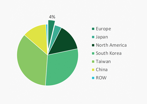
ASML system sales per region over the last 10 years. Credit: ASML/ BCG & SIA, 2020
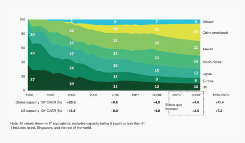
Global chip production capacity by region. Credit: ASML/ BCG & SIA, 2020
Thanks to lithography’s importance, a significant proportion of the funds announced will ultimately go to the world’s leading lithography equipment provider, ASML, based in Veldhoven, the Netherlands. As such the company published a position paper on the EU Chips Act quickly after its announcement in February 2022. While it ‘welcomes and strongly supports the European Commission’s proposal’, it also highlights the scale of the challenge of growing the region’s semiconductor market share to 20 per cent. It estimates that European total investment would have to be roughly $264bn to reach this level. Much may come from chipmakers, but they need government support to overcome the current ‘lack of advanced chip manufacturing experience on European soil’, ASML wrote.
‘We support Europe’s ambition to produce more advanced microchips in Europe,’ said Sander Hofman, ASML’s spokesperson and corporate communications manager. ‘In our view, the writing on the wall is clear. Demand for all kinds of chips will increase, so we welcome the return of government backing for our ecosystem at this crucial juncture. This initial investment may be a catalyst for more public and private investments in the coming years.’ He added that government investments in the basic and applied research areas fueling semiconductor innovation ‘are always welcome, as they are the fuel for big technology shifts like EUV’.
If you build demand, fabs will come
With the US also seeking to improve its home-grown semiconductor industry, one possible approach the Chips for America Act might take is developing a domestic rival to ASML. Hofman said that although the company is always vigilant about the semiconductor industry’s dynamics and development, it isn’t concerned about this. ‘At ASML, we see ourselves as system architects and integrators,’ Hofman said. ‘We have spent more than three decades building a strong global ecosystem of suppliers, partners, academia, institutes and customers that contribute to our innovation, pushing the boundaries of what’s possible. We can only pull off such feats of science and technology thanks to our ecosystem.’
All semiconductor innovators in the regions seeking to grow their market share must get involved, said Jo De Boeck, executive vice president and chief strategy officer at Imec, the Leuven, Belgium, semiconductor research centre. In Europe that will create ‘a very concerted action with a focus on building capacity’, he said. ‘The most important reason for doing pillar one is to get to pillar two, to make sure there’s more production globally, but also in the European market. Aiming at introducing more demand for the leading-edge nodes will become important for many applications in Europe in the future.’
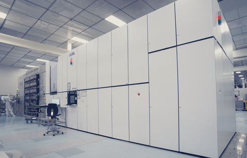
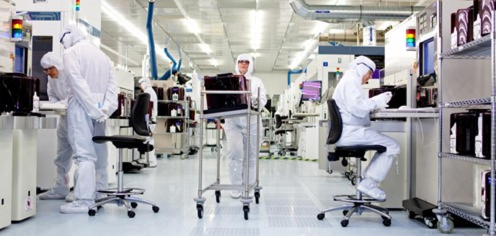
New Acts intended to incentivise the semiconductor industries in the EU and US will likely lead to investment in ASML’s leading-edge lithographic tools, like this one at Imec. Credit: Imec
De Boeck especially stressed that building more leading-edge fabs in the region requires effort to increase demand for the capabilities the resulting chips will offer. That will involve working to provide access to companies of all sizes and experience levels manufacturing products for, and offering services to, consumers. ‘If there is no demand, there is not going to be any economic decision to build a fab,’ De Boeck said. ‘So, pillar one will create a multitude of design centres across Europe, virtualising access to innovative pilot lines.’ In ‘every corner of Europe’, R&D teams will be able to ‘look ahead at the future, what the technologies can bring for their products and for their services’, De Boeck envisioned.
Doing this will not necessarily involve explaining lithography technology in detail. ‘They need to know there is something there that can enable them to scale functionality, or reduce their costs, or increase their efficiency,’ said De Boeck. ‘We need to make sure there’s access to the technology that makes the use case eminent.’ Such design enablement needs to happen at a very early stage, perhaps two generations before technology is commercialised, he added. Large chipmakers like Taiwan Semiconductor Manufacturing Company (TSMC) already do this, De Boeck said. And now, Imec wants to similarly ‘interface with the customers of our customers’.
Even though the vision of rebuilding semiconductor industries in Europe and the US are long term ones, they need to get started soon, De Boeck underlined. ‘2030 is some time away, but it’s coming fast because building fabs and building markets and market needs is an activity of years,’ he said. ‘So, we need to get our act together today to even come close to reaching the target.’ Europe may need $264bn of investment to reach a 20 per cent share of the semiconductor market as ASML suggests, but that can only be reached in stages by increasing demand, De Boeck said. ‘Doing nothing will definitely not bring any investments,’ he emphasised.