Is augmented reality (AR) going to happen? That was the question that colleagues of Xavier Lafosse, commercial technology director of advanced optics, at materials giant Corning asked him six years ago. Then, the company was just developing products for the market, and Lafosse was championing its potential. In 2020, that question has been answered by industrial and military users. ‘It has happened already,’ Lafosse said.
Getting to this stage has required crucial innovations in waveguides that direct images from a light engine, through transparent glasses, and from there into users’ eyes. To help achieve this, companies like Corning and glass manufacturer Schott have pushed glass melting, forming, and finishing technology further than ever before. Meanwhile, other companies, including Digilens and Sony, have developed potentially lighter, easier-to-shape plastic waveguides. Although the AR market has ‘happened already’ in Lafosse’s words, it is likely to grow if consumers adopt it widely. And in that case, each company’s differing approach will shape the optimal technology and manufacturing processes.
AR builds on Corning’s long-standing product line for vision-correcting spectacles, Lafosse explained, especially high refractive index glasses. ‘We’ve moved from very small preforms for the ophthalmic product into very large wafers, up to 300mm in diameter,’ he said. That has involved scaling up an entire supply chain to make glass extremely flat, as measured by total thickness variation (TTV) between opposite sides of a glass wafer. ‘TTV was improved to about an order of magnitude better,’ Lafosse said. ‘AR is the first application that requires such high flatness.’
To make AR devices, glass forms waveguides for display information, Lafosse said. Corning’s customers typically spin coat a UV-curing resin on top of such a wafer. Using processes such as nanoImprint lithography (NIL), they then imprint nanoscale features into the resin using a soft mould to produce gratings. Then, the manufacturer solidifies the polymer in a UV cure step, and removes the soft mould. Such gratings can couple light into the waveguide, create a two dimensional matrix of images, known as pupil replicas, and then couple light back out towards the user. Some challenges come specifically because of this design.
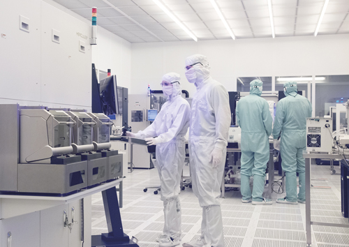
Nanoimprint lithography is already used in high-volume production on 200mm high refractive index glass wafers. Credit: EVG
‘Light is travelling sideways in the lens, meaning that the light path is going to be centimetres not millimetres,’ outlined Lafosse. Waveguiding designs differ between companies, with some using a different waveguide for each primary colour, and others transporting different colours in one waveguide. ‘After centimetres of light path there are some glasses where you could have up to 50 per cent of blue light absorbed,’ Lafosse said. ‘Our role has been to come up with glasses that are extremely pure to achieve this very high optical transmission, especially in the blue.’
Displaying potential
For waveguides, refractive index is a particularly important parameter, with high refractive indices needed to enable total internal reflection in waveguides. Light beams hitting the glass’s outer surface are reflected if the angle at which they arrive at the surface remains below a critical value, which is a function of the refractive index. Higher refractive indices therefore keep more light within the waveguide. In general, a higher refractive index also enables a wider field of view (FoV) in AR and mixed reality (MR) optics. However, Lafosse noted that FoV is sometimes traded off to achieve better image homogeneity. ‘Or you’ll see also people trading off FoV against a simpler design where they can combine all the colours into a single waveguide,’ he added.
Schott also provides glass wafers with diameters exceeding 200mm and refractive indices over 1.8, noted Michael Müller, the company’s PR and communication manager. ‘Wafer properties and wafer quality are superior due to process optimisation over the last couple of years and hundreds of thousands of Schott RealView glass wafers,’ Müller said. ‘Deeply immersive AR/MR applications are now possible, enabled by an FoV of up to 65°, based on a Schott RealView glass wafer with a refractive index of 1.9. AR/MR devices with a horizontal FoV of 53°, equal to 65° FoV diagonal, can be envisioned.’
The company’s refractive index 1.9 product also provides ‘crystal-clear image quality’, Müller added. ‘Schott RealView high-index glass wafers with a size below 300mm diameter are already proven in mass production,’ he explained. And now, a collaboration between Schott and semiconductor equipment supplier EV Group (EVG) has shown ‘supply chain readiness for 300mm high-refractive-index glass wafers while maintaining stringent specifications’.
At Photonics West in San Francisco, US, in February 2020, Schott and EVG teamed with resin supplier Inkron and AR display maker WaveOptics. Together they presented ‘the world’s first waveguides made on a glass substrate with a refractive index of 1.9 and a matching nanostructured polymer produced on a 300mm wafer platform ready for mass production’, said Müller. Schott’s RealView high-index glass wafer portfolio will enable WaveOptics’ latest generation of waveguides, named ‘Katana’, which weigh just 7g and are just 1.15mm thick, he added.
WaveOptics’ latest generation of waveguides, named Katana, weigh 7g and are 1.15mm thick
EVG’s deputy head of business development, Martin Eibelhuber, noted that reaching this stage has involved ‘incredibly fast’ progress. ‘It was our shared goal to combine all these very recent advances throughout the whole supply chain in a leading-edge waveguide design from WaveOptics,’ he said.
The collaboration exploited EVG’s SmartNIL technique for patterning UV-curing materials, in this case Inkron’s IOC-133 resist, deposited on Schott’s glass wafer. ‘It is a replication-based process that enables one to scale the patterning of complex optical structures to high volumes,’ Eibelhuber said. ‘From a preform, so-called master, it creates functional high-quality copies in such quantities that AR glasses can become an affordable consumer product.’
Clear diversity
EVG’s Hercules NIL tool receives blank wafers and resist materials as inputs and provides fully imprinted wafers with desired device structures as outputs, Eibelhuber explained. ‘The Hercules system takes care of all of the required pre-processing steps such as cleaning, resist coating and baking plus the SmartNIL process itself,’ he said.
Implementing new materials like Schott’s RealView wafers and Inkron’s resist in this process was a challenge, Eibelhuber admitted, but brought useful rewards. ‘We could immediately demonstrate a fully-integrated process on a real-world device,’ he said. ‘This finally resulted in fabricating 24 waveguides per single imprint with the highest refractive index materials available on the market.’ The outcome was partly a consequence of EVG’s NILPhotonics Competence Centre, which Eibelhuber called ‘a proven innovation incubator for the implementation of NIL’. ‘We cooperate with virtually all key players in the supply chain,’ he said.
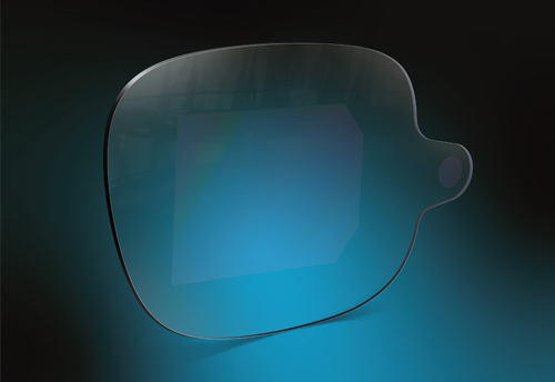
Augmented reality has driven the development of large high refractive index glass wafers. Credit: Corning
As such, SmartNIL technology is very insensitive to designs and enables many different waveguide formats. ‘This can be binary gratings, multi-level structures or even slanted gratings, and all of them have their specific challenges,’ Eibelhuber said. ‘Maybe more noteworthy is the fact that SmartNIL enables the scaling of the most complex structures in terms of volume and substrate sizes at the highest quality and performance. Together with our step-and-repeat mastering technology, it uniquely provides the capability to get the manufacturing done on highly efficient, state-of-the-art 300mm production lines.’
Among diverse AR waveguide designs, companies like Sony are developing them using plastic rather than glass. ‘Our plastic waveguide technology is for “usability in daily life”,’ explained Takuji Yoshida, senior device engineer at Sony’s R&D Centre in Tokyo, Japan. Requirements for such desirable products include light weight, a ‘socially acceptable’ form factor, design variation, and break-resistance. ‘We make AR glasses which have a more natural form and fashionable design like ordinary eyeglasses,’ Yoshida said.
To do this, Sony researchers have developed a ‘unique fabrication process of a full-colour plastic holographic waveguide combiner’. Many waveguides guide light using diffraction, but this can cause ‘rainbow’ effects where higher order diffraction degrades image quality. Holographic waveguides also offer better transparency, Yoshida suggested. ‘We employ a roll-to-roll process to produce the plastic holographic waveguide at room temperature, from the holographic optical element recording to the transfer process,’ he said. This used Bayfol HX photopolymer films manufactured by Covestro that did not require a heat process. ‘We potentially made it possible for the holographic waveguide combiner to be produced in mass-production at lower costs,’ Yoshida added.
Yet the advantages that plastic waveguides might bring are offset by some difficulties associated with the material. ‘A plastic substrate holographic waveguide combiner has been a challenge to make, because it has inherently insufficient optical flatness and birefringence,’ said Yoshida. Delivering successful designs therefore meant developing a way to injection mould optical grade plastic substrates. It also meant developing a hologram recording process that doesn’t use heat, and a holographic optical element (HOE) transfer process and precise alignment. Now the remaining optical challenges are to expand the FoV and to improve the utilisation efficiency of light, Yoshida said. ‘The FoV is about 25° in the diagonal,’ he said. ‘The eye box size is 9mm and 6mm in the horizontal and vertical fields of view, respectively.’ As such, Sony has not made any official announcements about commercialisation yet.
Constructing a supply chain
By contrast, Eibelhuber stressed that NIL-based methods are now making the transition from R&D to volume manufacturing. ‘Even though our SmartNIL technology is relatively young, it already has a proven high-volume manufacturing track record on 200mm wafers,’ he said. ‘Last year we launched the first fully integrated 300mm NIL track system, which is already being installed at first customer sites. We are convinced this is a breakthrough that will enable the required volume and cost targets of our customers.’
In this effort, EVG brings a wealth of NIL experience. ‘We have been working on NIL for more than 20 years and have explored many applications so far,’ said Eibelhuber. ‘Many of the process capabilities needed today have been developed during this journey and have been available for a while. However, as with many new technologies, it takes time to find the sweet spots for this technology to get out of the lab and into the fab. AR waveguides are a perfect example of an application ideally suited for NIL. For this reason, NIL has been an essential part of AR waveguide development since the early days.’
Nevertheless, the AR industry has not generally reached high production volumes, Müller conceded. ‘As the AR/MR industry is emerging, their needs for outstanding optical designs are emerging as well,’ he said. ‘Based on conversations with leading innovators in this industry, a supply chain for very demanding optical components is currently growing. This leads to improved optical engines, ever-better optical waveguides, as well as new coatings and resins.’
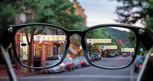
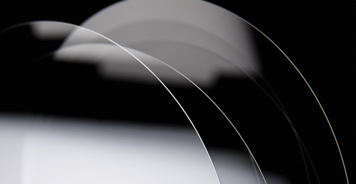
Innovations in waveguides look set to drive development of consumer AR. Credit: Corning
Müller argued that the Schott RealView portfolio offers versatile options for specific needs of the industry in mass production readiness. That means ‘our customers specify their needs, and we support them in reaching their goals, based on Schott RealView substrates’, Müller continued. ‘The supply chain includes the production of raw optical glass in Schott’s melting facilities in Germany, and processing in our facilities in Asia for steps like wafer cutting and polishing. In a final step, the resin and pattern needs to be added to the Schott RealView wafers. Here our customers have freedom of choice, whether they put the resins and patterns into the glass wafer by themselves on their machines, or contact a specialised processor who is capable of doing that.’
Corning, meanwhile, also supports customers by providing fully automated laser cutting tools to extract eyepieces, noted Lafosse. ‘From a manufacturing perspective, the overall ecosystem is really still building up,’ he added. ‘People are more focused on getting things right before actually making many of them. And we still need a lot of innovation to get to a cheaper, better product. I think the jury’s still out in terms of what’s going to be the winning technology from both a scalability and a cost perspective.’
Yet that innovation is happening fast. ‘There’s not a week where we don’t see more adoption from large companies,’ Lafosse said. ‘We believe at this point that we’ll see consumer products in 2023, maybe 2024. But it will take time to get to the right form factor and performance.’