Last year, scientists at the University of Rochester’s Institute of Optics published a paper introducing the concept of a metaform – a freeform optical element imprinted with millions of nanoscale structures that make up a metasurface.
The structures on a metasurface function like optical antennae, which, through their design, shape how light interacts with the surface. The researchers state, to the best of their knowledge, this was the first time a metasurface had been applied to a freeform imaging element, in this case a mirror – metasurfaces are normally written on flat surfaces.
The work opens the door to creating new types of optical components with unique properties. This particular metaform optic was designed as a combiner for a near-eye display in AR/VR glasses, to direct light efficiently into the eye.
Metasurfaces are finding uses in various fields, from sensing in medicine to imaging. In November last year, researchers at Princeton University and the University of Washington published work in Nature Communications presenting an imager the size of a coarse grain of salt. It’s a nano-optics imager based on a metasurface with 1.6 million cylindrical posts, but the achievement is that it’s able to produce images on par with a conventional compound camera lens, all through the use of neural networks to reconstruct the images.
One of the difficulties of working with metasurfaces is to design and configure the nano-structures to get the desired output. From an optical modelling standpoint, metasurfaces present a challenge of scale.
As Chenglin Xu, product manager of RSoft photonic device tools at Synopsys, noted, metasurfaces are usually big – up to millimetres in size – but contain millions of subwavelength nano-atoms. The nanometre-scale structures would typically be modelled with electromagnetic solvers like finite-difference time-domain (FDTD) and rigorous coupled-wave algorithm (RCWA), but using these for the entire structure would take too much computer memory and computation time. ‘Even with stitched FDTD, a millimetre-size metasurface can take weeks to simulate on the cloud with thousands of nodes,’ Xu said. ‘This makes optimisation, which requires a vast number of simulations, virtually impossible.’
This was one of the problems the University of Rochester team faced when designing its metaform optic, which measured around 2.5mm across. Daniel Nikolov, optical engineer at the University of Rochester’s Institute of Optics, and lead author of the metaform optics paper in Science Advances, explained: ‘Being able to have a simulation that can account for the complete optic – which is on the scale of millimetres in our scenario – while having precision in the simulation to resolve the light-matter interactions at a scale of nanometres is prohibitively expensive in computational power and time. So you have to figure out some smart ways to bridge the two scales.’
The University of Rochester team combined different software tools. They used Code V from Synopsys for ray tracing, to calculate the phase response needed to get a good image. They then used Lumerical FDTD software to model what kind of metasurface was required to achieve that phase.
Nikolov said: ‘There’s still a lot of space for improvement when integrating metasurfaces in optical design, and that’s something that the field as a whole is starting to tackle. If you try to combine traditional imaging optics and new types of devices like metasurfaces, you have to be smart about how you model them.’
Xu said that, when working with metasurfaces, designers have to make some assumptions and use the most feasible approach based on the application. He said there is no single approach that works for all applications and each one has its advantages and disadvantages. He also advised decoupling a big and complex problem into a number of small problems at different levels and solving them individually, using different tools.
Weighing up the pros and cons
Finite-difference time-domain (FDTD) is the most rigorous approach to modelling metasurfaces, according to Xu, but is only applicable to very small structures because of the amount of computer memory and computation time required. On the other hand, ray tracing is fastest, Xu explained, but does not take coherence and diffraction into account, and thus cannot be applied to any off-state operation with phase discontinuities that cause diffraction.
Another option is finite-difference beam propagation method (FD-BPM), which, Xu said, is an efficient algorithm for large metasurfaces and requires less memory than FDTD. However, since BPM traces wave propagation in only one direction, Xu noted that it is best used for large metasurfaces with negligible reflection.
For large metasurfaces with significant reflection or resonance, Xu suggested a combination of fast Fourier transform (FFT) BPM with a transfer function mask (TFM) as being the best approach. He explained that this is because, firstly, TFM is the surface property of the metasurface and reflection or resonance has been taken into account; and secondly, FFT-BPM is the exact solution in a free space or homogeneous medium: ‘Like any other approach, FFT-BPM plus TFM has its limitations,’ he said, ‘such as ignoring high-order diffraction or neighbour coupling among meta-atoms because of the locally periodic assumption in obtaining TFM.’
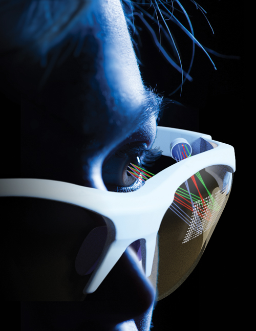
The University of Rochester’s metaform optic was designed as a combiner for a near-eye display in AR/VR glasses. Credit: University of Rochester / Michael Osadciw
TFM can be constructed with rigorous electromagnetic solvers, such as FDTD or RCWA. Xu said that RCWA is at least 10 times faster than FDTD, although Nikolov noted that RCWA is limited to periodic structures such as linear gratings. For any metasurface with a more complex phase, such as a lens, FDTD is used, Nikolov said.
Synopsys provides design and simulation tools with these algorithms, including FDTD-based FullWave, BPM-based BeamProp, RCWA-based DiffractMOD, and ray tracing-based Code V.
More than optimisation
Nikolov said that, when thinking about the metaform optic, it was important that modelling wasn’t treated as just a theoretical optimisation problem. ‘We always knew this was going to be an experimental proof-of-concept device,’ he said. ‘The key was to keep in mind the complete process chain – from design to fabrication and testing. In considering the complete pipeline we constrained the modelling software in such a way that the device can still be manufactured and validated.’
Writing a metasurface on a curved optic had not been done before, and the University of Rochester team wanted to make sure the metaform could actually be manufactured.
‘In typical optical design software there are tools for tolerancing,’ Nikolov continued. ‘You can specify how much the system parameters may change during fabrication and the optical design software can evaluate how that will affect performance. The modelling methods for metasurfaces are not at that level of automation yet, so we had to manually evaluate the performance cost of various manufacturing errors and limitations.’
As an example, the team calculated the smallest feature that could be written on the mirror, and then constrained the metasurface features to be larger than that in the design solution space. They also analysed how variation in the sharpness of the corners of nano-structures would affect performance.
To make nano-structures tolerant to manufacturing errors, Xu advised that, within the subwavelength pitch, the meta-atom cannot be too small to manufacture, but it also cannot be too big, since this could result in a gap that is too small to make. He said that the meta-atoms’ possible dimensions range has to be extensive enough to provide a 360° phase delay; otherwise, the meta-atoms have to be high enough and this makes fabrication more difficult.
His second piece of advice for designing metasurfaces is to choose a shape of meta-atom that has a performance that is less sensitive to manufacturing errors. For example, waveguide-based nano-pillars or holes are more tolerant to resonance-based coupled nano-cells, he said.
Nikolov said: ‘If metasurfaces are to become part of consumer technology, or devices that are going to be produced on a larger scale, yield is very important. What matters for yield is how sensitive the design is to tolerances.’ This would certainly be the case for an optical element for virtual reality glasses.
‘The [modelling] method that we chose has its benefits but also its limitations,’ Nikolov added. ‘We’re exploring new avenues to advance the design, the fabrication, and the testing.’
Improving and optimising spectrometer designs
Spectroscopy is the study of the emission and absorption of light. A spectrometer is a device that splits light into its component wavelengths, typically using a grating, and then measures the power/energy of the light as a function of wavelength.
The detector can be either a single element, a 1D or a 2D array detector. There are numerous types of spectrometers such as Czerny-Turner, crossed Czerny-Turner, concave grating, fluorescence, and many other types. Spectrometers can also be either reflective or transmissive.
Spectrometers can be designed by hand using calculations and basic raytracing, and have been designed this way for many years. Using model optical design and analysis allows these designs to be improved for higher performance and efficiency. Factors such as stray light are also much more easily analysed and corrected in the software environment.
Lambda Research Corporation’s TracePro and OSLO optical design and analysis software products give the optical engineer, designer, or scientist the tools they need to design, optimise, and analyse many different types of spectrometers, both reflective and transmissive. OSLO is an excellent choice for the design and optimisation of the optical elements in the spectrometer, including collimating, focusing, and turning mirrors. Figure 1 shows a concave grating spectrometer in OSLO.
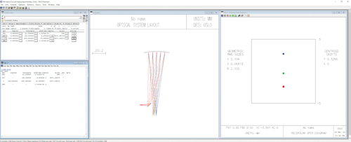
Figure 1. Curved grating spectrometer in OSLO
TracePro can be used for additional optical and opto-mechanical design and analysis of a spectrometer. The optical design can be imported from OSLO or developed and optimised directly in TracePro. The mechanical and opto-mechanical elements can be imported from a CAD program or added in TracePro, using TracePro’s built-in CAD modelling tools. Figure 2 shows a concave grating spectrometer similar to the OSLO model above, in TracePro. This spectrometer uses a fibre optic cable for optical input and a turn mirror to direct the light to the concave grating. The detector in this spectrometer is a linear array detector.
Once the spectrometer model has been built, properties can be applied to the model and light sources defined. Examples of properties applied are reflectivity and scattering parameters for the two mirrors, and absorption and scattering for the coatings inside the spectrometer. Other parameters such as absorption, transmission, and reflectivity of the detector and detector window can also be modelled. Many of these parameters can vary as a function of wavelength, incident angle, and temperature. These factors can play a significant role in the final performance of the spectrometer. The user can then analyse the performance metrics of the system, such as throughput, dispersion, and stray light.
Figure 2 shows the specular rays in the spectrometer. These are the rays that a designer wants to hit the detector. If the analysis was stopped at this point it could be assumed that the spectrometer will function as expected. In some cases, this level of performance may be acceptable, but in others higher performance may be required.
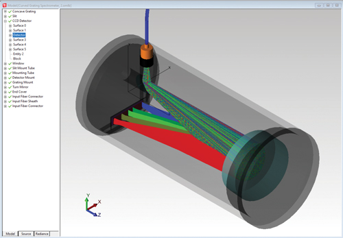
Figure 2. Concave grating spectrometer in TracePro
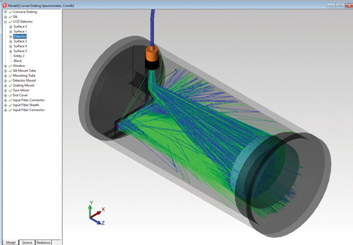
Figure 3. Stray light in the spectrometer
Figure 3 shows specular and scattered rays striking the detector. This image shows that many more rays than just the specular rays make it to the detector. These extra rays would be considered stray light. Figure 4 shows the irradiance map for the detector. This plot is in a log scale. Note the noise floor due to stray light at around 3.16 W/m2. This will serve to reduce the dynamic range of the system. Ideally this background noise should be as low as possible.
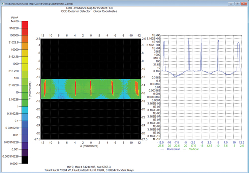
Figure 4. Irradiance on detector surface
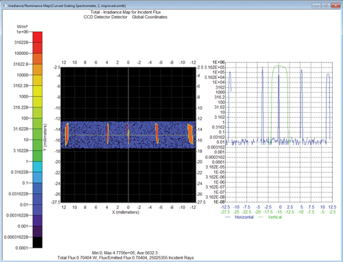
Figure 5. Irradiance map on detector after changes
A big advantage of designing and optimising devices such as spectrometers in a virtual environment, such as TracePro or OSLO, is the ability to try many variations in a short period of time. The effects of changing some of the parameters of the design can easily be evaluated and quantified. For example, the mirror finish can be improved, an anti-reflective coating added to the window in front of the detector, and the black coating inside the spectrometer can be changed to a better one. The results of these changes can be seen in Figure 5. Note that the noise floor is now 0.01 W/m2, a factor of more than 300x improvement. This will improve the dynamic range of the spectrometer.
Once the designer is satisfied with the design, the model can be exported in a CAD format that can then be used in the designer’s CAD program to make production and assembly drawings.
TracePro and OSLO give the user the ability to analyse numerous designs and solve most problems in a virtual prototyping environment, before committing to actual hardware prototypes. This can speed the development process and reduce the overall design and development costs.