Nanoelectronics research hub Imec is partnering with KMLabs, a specialist in ultrafast laser and EUV technology, to establish a real-time functional imaging and interference lithography laboratory.
This lab will enable imaging in resist on 300mm wafers down to an 8nm pitch, in addition to time-resolved nanoscale characterisation of complex materials and processes - such as photoresist radiation chemistry, two-dimensional materials, nanostructured systems and devices, and emergent quantum materials.
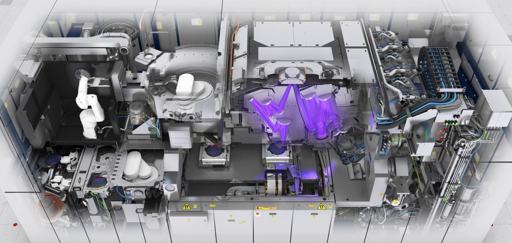
EUV holds the potential for transforming semiconductor manufacturing by allowing chipmakers to produce finer features in single step layers that would otherwise require multiple exposures, reducing the cost of manufacturing significantly. However, the commercial deployment of EUV lithography has been hit by years of delays, mainly due to the engineering challenges associated with creating EUV systems bright and reliable enough to operate in fabs 24 hours a day, 365 days a year.
Part of this challenge results from a lack of fundamental understanding of EUV sub-picosecond exposure processes, according to Imec researchers. Being the 'first industrial lab to do so', Imec’s attolab will enable the study of EUV photon absorption and subsequent ionisation processes at unprecedented timescales from attoseconds to picoseconds. It is anticipated that the gain in fundamental understanding of material characteristics pave the way for the development of new lithographic materials and underlayers.
These capabilities expand upon Imec’s post process analysis capability and will allow the characterisation of the molecular and quantum dynamics of materials within the attosecond to picosecond (10-18 s to 10-12 s) time regime, as well as to image lithographic feature sizes that far exceed the technology roadmap.
Because of the coherence of KMLabs’ high-flux source, Imec’s attolab will also enable interference imaging to emulate high numerical aperture (NA) imaging at 13.5nm. By combining the interference emulation of the 0.55NA of ASML’s most advanced tool in development with the current EUV scanner in Imec’s cleanroom, Imec and its partners will be able to explore the fundamental dynamics of photoresist imaging before the 0.55NA tools become available. The 300mm interference lithography (IL) capability will allow them to study advanced patterning films and processes using state-of-the art metrology tools, and will continue to be used to extend the knowledge of resist physics and chemistries to the very limits of material science.
While initially setting out to aid the development of next-generation EUV lithography tools, many other research areas will benefit from such a facility. Beyond molecular dynamics and ionisation processes of imaging materials, this lab will also provide the ability to do attosecond time-resolved electron spectroscopy and imaging of materials in an industrial setting. This is essential to accelerate the development of future logic, memory, and quantum devices, and of next-generation metrology and inspection techniques.
The new laboratory will be equipped with multiple KMLabs EUV beamlines, providing the platform for a jointly developed series of EUV end stations.
'Bringing this high-NA exposure and attosecond analytic capability to imec’s 300mm cleanroom will enable unprecedented fundamental learning, significantly speed up cycles of learning, and positively impact the semiconductor technology roadmap in many critical domains,' Greg McIntyre, director of advanced patterning at imec.
'Stochastic defectivity, resist photochemistry, and novel electronic materials development are all critical to the next generation of semiconductor enablement. KMLabs is proud to work with imec on system development, advanced metrology, and solutions in these areas,' added Dr Kevin Fahey, CEO KMLabs.
Image: The inside of an EUV lithography system. Credit: Imec
