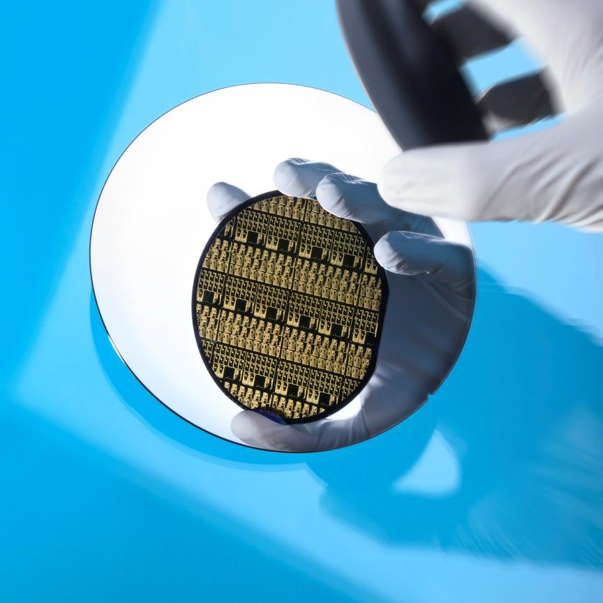
After decades in development, the era of manufacturing silicon chips through lithographic methods using extreme ultraviolet (EUV) light is finally here. South Korean giant Samsung has claimed readiness to use EUV tools in manufacturing first, scheduling production before the end of 2018.
The move is needed to deliver on the Moore’s Law promise of continuously shrinking transistors – and thereby improving processor performance – to what’s known as the 7nm node. Among other leading silicon chip producers, Taiwan Semiconductor Manufacturing Co (TSMC) and California-based GlobalFoundries are intending to start commercial 7nm EUV production early next year. That’s the same timing that Intel plans for 10nm node production – despite the company being founded by Gordon Moore, after who the famous law is named. The fact that it’s behind the others may be a strategic decision, or it may be because it’s struggling with the complexity of introducing EUV.
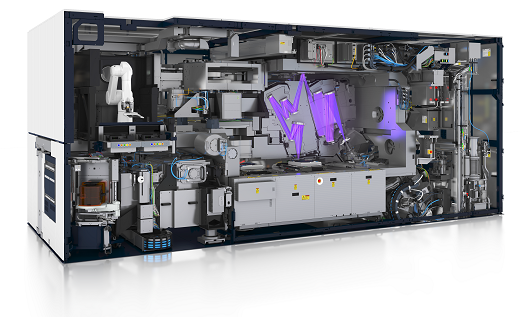
Marco Pieters, vice president EUV product marketing at ASML, which supplies EUV scanners to all these companies, declined to comment on specific customers’ activities. ASML’s scanners expose photoresist material coated onto silicon wafers to EUV, hardening them, before engineers wash away the unexposed material. The remaining shapes define the components, which workers etch out with acid later in the process. Pieters emphasises that scaling down ‘circuits, devices, geometries and architectures’ drives semiconductor industry growth. ‘Chipmakers are introducing EUV lithography in volume manufacturing because it delivers cost reductions, device power savings and further device performance improvements well into the next decade,’ Pieters noted.
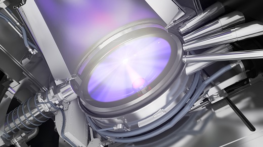
A critical element in reaching this stage has been developing a laser source that can make 13.5nm light. The current approach fires a stream of microscopic droplets of molten tin into a vacuum chamber, where two laser blasts strike each of them sequentially. The first flattens the droplets into a pancake shape, and the second high-power blast vaporises them, emitting EUV light.
To qualify EUV scanners in high volume manufacturing, device makers needed 250W of laser source power, explained Meng Lee, director of product marketing at Veeco, a process equipment supplier based in New York. ‘This is required to achieve 125 wafers an hour. This was considered as the primary inflection point of EUV lithography adoption, as the device makers began to see the cost impact and limitation of optical projection lithography, especially on the 7nm node.’
‘The challenge has been to get higher powers reliably and consistently,’ commented ASML’s Pieters, to achieve such productivity levels. He said ASML has worked tirelessly to improve uptime by improving components like the tin droplet generator. Its TwinScan NXE:3400B EUV scanner therefore met high volume manufacturing specifications in 2017. ‘The EUV source has seen 20 years of development,’ Pieters said. ‘We know that this technology is scalable and will enable EUV in high volume chip manufacturing. In our San Diego research labs, we have demonstrated a viable path towards 375W source power.’
Reflective outlook
The change in wavelength for EUV lithography also leads to other major process changes. ‘EUV light is absorbed by everything, even air,’ observed Pieters. Therefore, exposure steps are done in vacuum, while using mirror rather than lens optics. The masks that outline the minute, highly complex, patterns that the scanners form on photoresist also need to be moved in and out of vacuum quickly and cleanly. Altogether the shift to EUV ‘requires an entirely new manufacturing process, using different kinds of materials, to get the right accuracy and cleanliness’, Pieters said.
‘The industry has come a long way in getting all the major issues behind us to justify the shift from transmissive to reflective masks,’ Veeco’s Lee remarked. Other areas now need attention to improve yield on next generation nodes, including defects in the mask blanks, the master plates used to transfer patterns onto silicon wafers. New mask inspection techniques using short-wavelength actinic light must come into broad use to allow the adoption of pellicles that protect EUV masks from particle contamination, Lee added. However, while this absence affects yield and cost, it doesn’t damage the technology’s fundamental viability. Current technologies are ‘good enough to get started and not to fail on the 7nm node’, said Lee, and Veeco’s tools have qualified for this use.
ASML's EUV lithography tools make 13.5nm light by firing microscopic droplets of molten tin into a vacuum chamber, where laser blasts stike them. (Image: ASML)
Veeco supplies ion beam deposition tools that produce mask blanks. Its tools deposit multiple layers of molybdenum and silicon to form reflective masks, plus ruthenium capping layers that protect underlying layers from oxidation and degradation by the EUV light. Lee said that the company is building tools to accommodate device maker ramp-ups. ‘We are also actively working with our customers and device makers to align technologies to address the 5nm technology node and beyond,’ he added. Veeco is also developing deposition and etch processes for thinner absorber layers used to define the mask areas that should not reflect the EUV light. Nickel, cobalt and related alloys might produce clearer images than existing tantalum nitride (TaN) absorbers, Lee suggested, because the newer materials can make thinner absorbers, and reduce problems caused by the shadows TaN casts.
The reason that reducing wavelengths in optical projection lithography is worthwhile is captured by the Rayleigh criterion, the formula that sets the minimum physical limit for resolvable detail. Written as k1ë/NA, the formula has three moving parts. The most fundamental are the wavelength, ë, and numerical aperture, NA, which characterises the range of angles over which the system can emit light. The technology factor, k1, depends on process-specific factors like the illumination geometry, the lithographic mask technology and the photoresist used in the process. Steps like reducing k1 and increasing NA have allowed 193nm immersion lithography to persist until the 7nm node. Jumping to a lower wavelength has become the best way to push the resolution limit down further – but the other factors remain important.
Great contrast
Reducing k1 in EUV processes means correcting for a multitude of process variables, Pieters noted, which ASML addresses with its Holistic Lithography product portfolio. That includes the company’s lithography systems, ‘which themselves are already highly configurable and flexible’, Pieters stressed. It integrates them with optical and e-beam metrology solutions that analyse and control the manufacturing process in real-time and advanced computational modelling that develops, predicts and optimises the process. Its system also helps avoid undesirable imaging artefacts caused by reflection and diffraction from EUV masks, known together as 3D mask effects. ‘Our computational lithography products in optical proximity correction (OPC) and source-mask optimisation (SMO) help minimise 3D mask effects as much as possible,’ Pieters added.
Numerical aperture (NA) on first-generation tools is around 0.33, but ASML is developing a next-generation EUV platform increasing this to 0.55. ‘This platform, which has a novel optics design and significantly faster stages, will enable scaling beyond the next decade, offering a resolution and overlay capability that is 70 per cent better than today’s most advanced EUV systems,’ Pieters said. The key to delivering high-NA optics ‘lies in their larger sizing, multi-layered design, and extreme smoothness requirements’ Pieters said. ‘If you were to blow up a high NA mirror to the size of planet Earth, the biggest aberration would be the size of a human hair.’
These optics are made by ASML’s partner Zeiss Semiconductor Manufacturing Technology (SMT) in Oberkochen, Germany. Winfried Kaiser, Zeiss fellow and senior vice president product strategy of SMT, explained that the EUV lithography optical system consists of projection optics and an illumination system. Zeiss produces the complete EUV lithography optical systems, which are ‘an essential part of ASML’s EUV wafer scanners’. To reduce the k1 figure it’s important to form high contrast images on the photoresist, Kaiser explained. ‘We achieve this key requirement through extremely low aberrations in the projection optics.’ Zeiss’ illumination system results in high image contrast and allows customer-specific imaging optimisation, he added.
Kaiser said that getting to a 0.55 NA requires ‘innovative multi-mirror design of the projection optics’. ‘Of the same importance is the technology to produce the extremely precise mirror surfaces – especially the new metrology and polishing technology,’ he added. As well as increasing the angular range coming from the illumination system, the angle of incidence of radiation on the mask is important, because it impacts 3D mask effects. Zeiss’s task is therefore ‘to ensure that the angles on the mask remain within narrow limits when designing the system in order to keep the 3D effects acceptable’, Kaiser underlined.
Increasing NA therefore means resolving 3D mask effects, notes Andreas Erdmann, group manager at Fraunhofer Institute for Integrated Systems and Device Technology (IISB) in Erlangen, Germany. ‘ASML and Zeiss have proposed to increase the demagnification in the scanning direction, which will reduce angular spread on the mask side,’ Erdmann said. ‘Demagnification in the direction perpendicular to the scanning will stay at 4x, which helps to keep the throughput.’ Changing demagnification helps resolve 3D mask effects such as non-telecentricity, where the image formed by an illumination system moves if it goes out of focus. ‘You have to create images all over the back of the photoresist,’ Erdmann explained. ‘If you have a slight variation of the focus, your images are created at different positions. You can tolerate this to a certain degree, but not completely.’
Producing answers
Erdmann studies 3D mask effects closely, helping develop mitigation strategies. ‘Thinner but stronger absorbing materials can help to reduce mask induced non-telecentricity, contrast fading and feature dependent shifts of the best focus position,’ he said. ‘However, potential candidate materials are difficult to process and repair with existing technology.’ He noted that attenuated phase shift masks that use thin absorber layers in locations where UV light shouldn’t be reflected are a possibility.
Reducing k1 will likely involve resolution enhancements from previous lithographic nodes, Erdmann added. ‘This includes advanced off-axis illumination schemes, OPC, phase shift masks, computational lithography and others,’ he explained. ‘EUV can be also combined with double patterning schemes which enable k1 factors below 0.25, the theoretical limit for dense patterns. It is important to note that there is not a single best solution or combination of mask and illumination settings. Appropriate compromise solutions have to be found. Combinations of predictive models and multi-objective optimisation techniques will support users to identify such solutions.’
First-generation tools have a numerical aperture of 0.33, but ASML is developing a platform to increase this to 0.55. (Image: ASML)
Zeiss already offers products to resolve some issues, noted Kaiser, such as mask repair system MeRiT neXT, mask tuning system ForTune EUV and metrology system Prove neXT. ‘Zeiss offers with AIMS EUV [an inspection tool] the industry platform for the actinic review of EUV photomasks, which provides full emulation of the EUV scanner,’ he said. ‘The first system has already been shipped to a customer more than one year ago.’
And despite the challenges that the shift to EUV poses, early throughput challenges are offset by fundamental advantages, Kaiser said. ‘One EUV layer can replace a double or triple exposure with immersion lithography,’ he said. ‘This double or triple exposure typically consists of several process steps, so that EUV can effectively reduce the number of process steps in semiconductor production by significant factors with just one EUV exposure.’
Single exposure EUV imaging on critical layers typically means processes use around a third of the number of steps that previous nodes did, ASML’s Pieters remarked. Consequently, ASML sees customers bringing EUV lithography into high volume manufacturing for the 7nm logic node, he noted. ASML is committed to making tools that process more than 125 wafers per hour that are available for volume manufacturing more than 90 per cent of the time, Pieters added. Meanwhile, the company continues to build capabilities to support a larger installed base. ‘We shipped 10 EUV systems last year, we have planned shipments of 20 systems in 2018 and we have a production capacity of at least 30 systems in 2019,’ he said.
By expanding from these modest numbers ASML shows that it is overcoming the sheer difficulty of developing the technology. ‘EUV lithography has been a long road with formidable challenges along the way,’ Pieters stressed. ‘We have had to bridge the gap between understanding its fundamental physics and engineering an industrial system that can produce chips in the high volume fabs of our customers.’
First image: EUV lithography optic illumination system made by Zeiss. (Image: Zeiss)