Japanese scientists have investigated how the properties of laser-induced periodic surface structure (LIPSS) are affected by the type of laser producing them.
The work, published in Scientific Reports, is intended to further encourage the widespread application of LIPSS to achieve simple, cost-effective and accessible fabrication of nanostructured surfaces in optoelectronic device production.
The ability to create structures on sub-micron scales is vital for producing the transistors and other constituents used in optoelectronic devices, which continue to shrink as demand for additional computing power, storage, and energy efficiency grows.
Currently such fabrication is being addressed via methods such as photolithography and e-beam lithography, however these are known to be complicated, extremely expensive, generally inaccessible, and requiring high levels of expertise.
LIPSS have been earmarked as a novel and prospective alternative to such methods. Here, femtosecond lasers are used to deliver ultrashort laser pulses that spontaneously lead to the formation of periodic patterns on the surface that are much smaller than the laser wavelength.
To achieve more standardised production of LIPSS – with controllable properties and characteristics for specific applications – it is critical to understand how the laser source used affects the quality of the formed surface structure, namely in terms of the crystallinity of the substrate and the potential for defects and strain.
To achieve this, a Japanese research collaboration led by scientists from Nagoya Institute of Technology, in partnership with Osaka University, Tokai University, Kyoto University, and the Japan Atomic Energy Agency (JAEA), has now directly investigated the various parameters that are influenced by the choice of laser source.
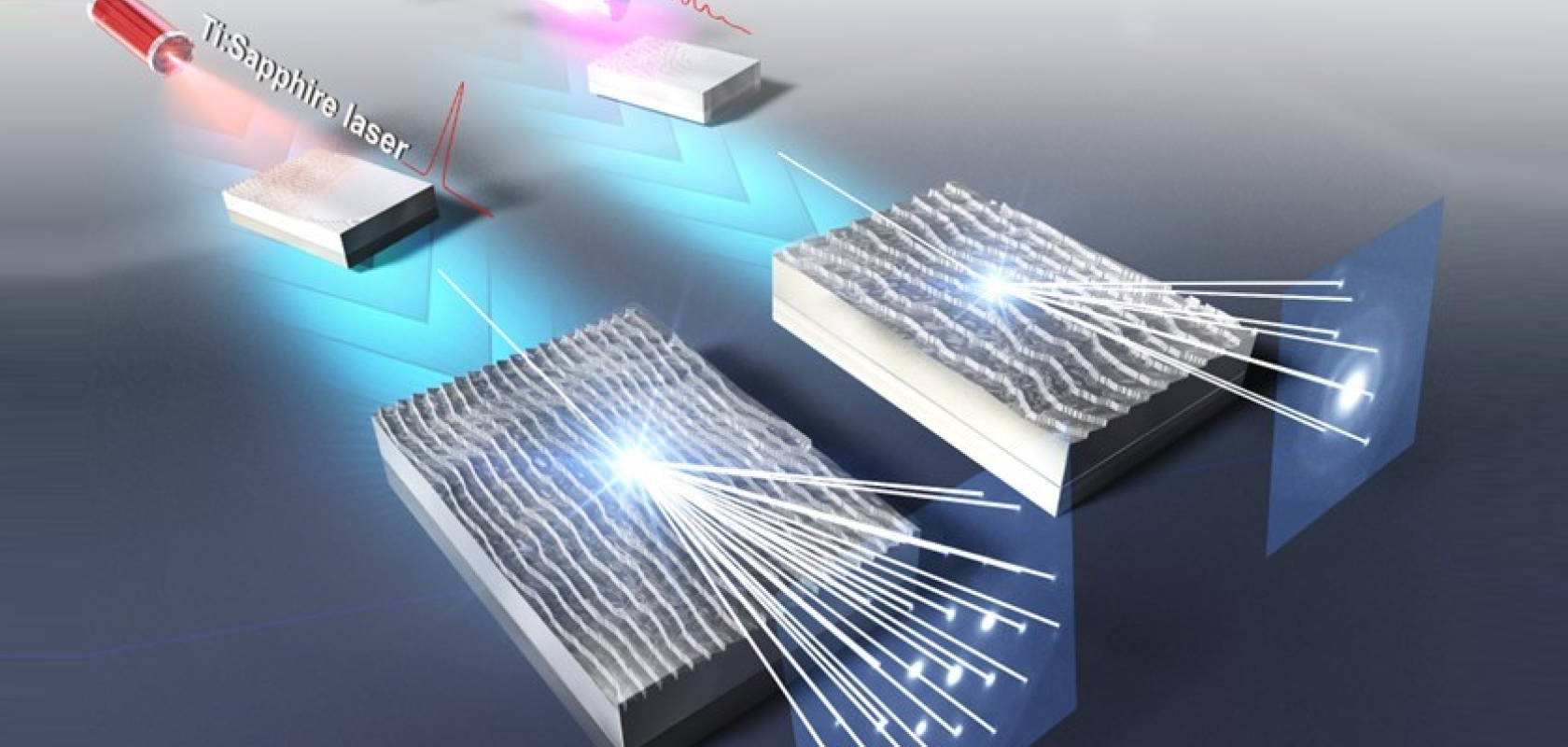
The scientists used two different femtosecond lasers on a silicon substrate – a material used in many optoelectronic devices. In one experiment, a Ti:Sapphire laser with a wavelength of 0.8µm was used to structure the silicon at higher than the band-gap energy. In another experiment, a free-electron laser was used with a wavelength of 11.4µm (mid-infrared), which could in contrast probe the effect when the energies are lower than the sample band-gap energy.
The analysis of the produced LIPSS samples was done both microscopically and macroscopically. The microscopic crystallinity and purity were studied using transmission electron microscopy (TEM), while a more macroscopic analysis of the strain and stability of the wider structure was investigated using synchrotron high-energy x-ray diffraction.
“When the Ti:Sapphire laser was used, the observed LIPSS retained the highly crystalline nature of the silicon but seemed to take on some residual strain,” said Dr Reina Miyagawa of Nagoya Institute of Technology. “In contrast, the LIPSS that were formed by the mid-infrared free-electron laser led to some clearly visible defects. However, there was no observable strain to the system whatsoever.”
The findings indicate how LIPSS can be tuned and tailored for specific applications by manipulating their defects, strain, and periodicity, through an appropriate choice of laser. According to the researchers, continued research along these lines will further open the pathway towards the widespread application of LIPSS in order to to achieve the cost-effective, simple, and accessible fabrication of nanostructured surfaces for applications in a wide range of optoelectronic devices.
