Researchers have created a photonic chip that can be produced and programmed without using complex and expensive lithography methods.
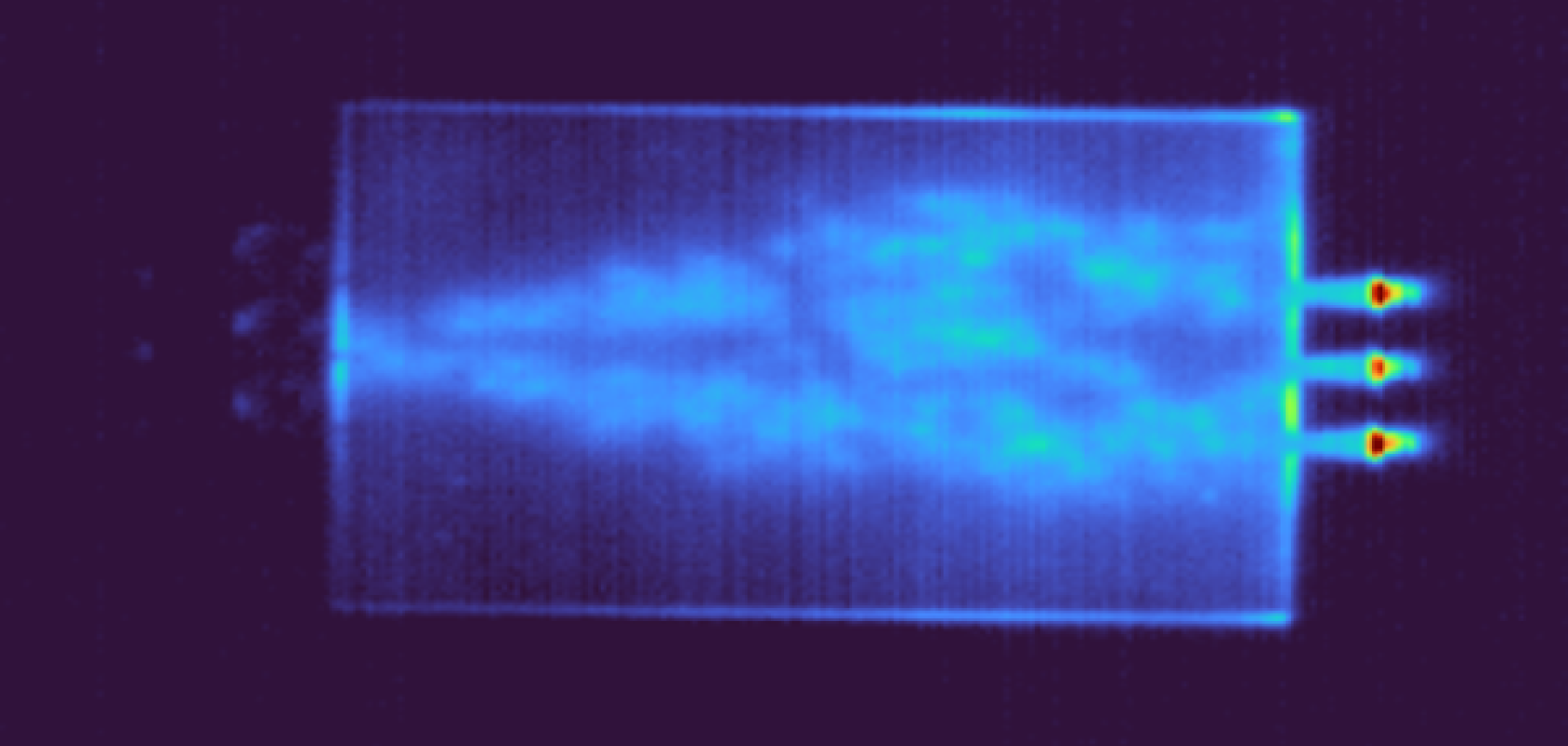
Described in Nature Photonics, lasers can be cast directly onto the device – a simple semiconductor wafer – in dynamically programmable patterns to reconfigure its computing functions as a photonic information processor.
The ability to reprogram the chip this way is critical for real-time machine learning and AI, the researchers say.
Photonic microchips can process information at the speed of light without losing energy or generating heat, which makes them better suited than electronic circuits for data-hungry AI applications.
However, like electronic circuits, photonic chips typically rely on complex lithography to define their circuit elements and connect them sequentially, which means they can be difficult to make. But the researchers say their device changes this.
“Photonic chips intended for machine learning applications face the obstacles of an intricate fabrication process where lithographic patterning is fixed, limited in reprogrammability, subject to error or damage and expensive," says Professor Liang Feng, from the University of Pennsylvania School of Engineering and Applied Science. "By removing the need for lithography, we are creating a new paradigm. Our chip overcomes those obstacles and offers improved accuracy and ultimate reconfigurability given the elimination of all kinds of constraints from predefined features."
Because there are no pre-defined lithographic patterns, the team says the device is inherently defect-free and can adjust its laser-cast patterns to handle tasks of varying complexity.
PhD student Tianwei Wu explains: "We can build and use [the device] very quickly. We can integrate it easily with classical electronics. And we can reprogram it, changing the laser patterns on the fly to achieve real-time reconfigurable computing for on-chip training of an AI network."
"The interesting part," says postdoctoral fellow Marco Menarini, "is how we are controlling the light. Conventional photonic chips are technologies based on passive material, meaning its material scatters light, bouncing it back and forth. Our material is active. The beam of pumping light modifies the material such that when the signal beam arrives, it can release energy and increase the amplitude of signals."
Feng compares the device to a pen: "Pumping light is our pen to draw the photonic computational network (the picture) on a piece of unpatterned semiconductor wafer (the blank page)." However, according to the researchers, unlike indelible lines of ink, these beams of light can be drawn and redrawn to deliver the re-programmable functionality.
Learn more about the new device in Nature Photonics.