Skip to main content
Social media links EO
LinkedIn
Twitter
Log in
Register
Applications
Life sciences
Environment
Quantum
Defence
Automotive
Aerospace
Medical engineering
Electronics
Optical communication
Technologies
Illumination & energy
Imaging
Industrial lasers
Lasers & optoelectronics
Sensors, test & measurement
Photonics 100
UK Photonics
Photonics Frontiers
Resources
Webcasts
White Papers
Supplier
Events
Products
Search
EU funds new Finnish chips competence centre
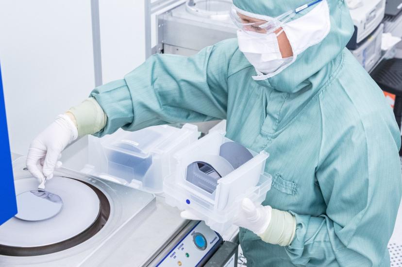
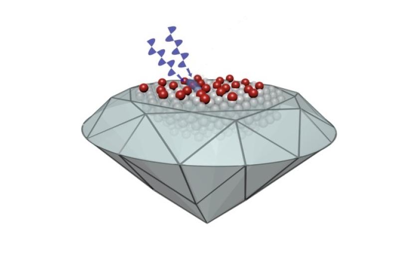
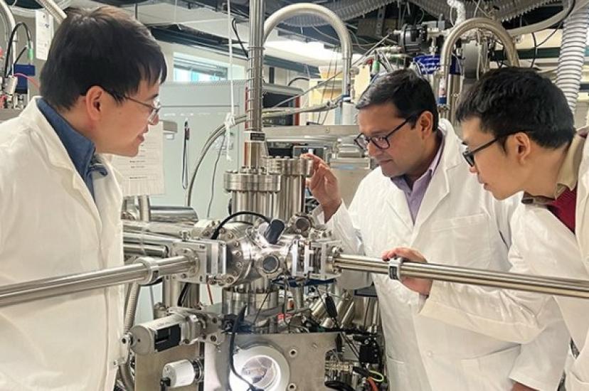
Diamond semiconductors? Laser method achieves atomic-scale precision on surfaces
Lightmatter and Amkor collaborate to deliver largest 3D-packaged photonic chip for AI
Transparent semiconductor material enables optical devices in harsh environments
How will the EU's photonic chip pilot line boost PIC capabilities in Europe?
Infinera's CTO's insights on the global supplier of products for telecommunications networks
Political figureheads visit imec's research centre ahead of the opening of Spanish facility
Saïd Rouifed
New ZEISS President and CEO set to step into role in 2025
IBM open first quantum data centre in Europe and expand operations in U.S
Pagination
Previous page
‹‹
Page 12
Next page
››
Media Partners
")


")
 will succeed Dr. Karl Lamprecht (right) in 2025 (Image: Zeiss)")
")