The properties of chalcogenide glass optics have opened up a number of use cases in infrared optics applications and beyond. This article assesses how some of the associated manufacturing and handling challenges of this material can be overcome
Use cases for infrared optics have exploded in recent years, with applications as far-reaching as thermal imaging, machine vision, home security, autonomous vehicles, astronomy, food safety and healthcare, to name just a few.
The optical performance of lenses used for devices in these applications are critical, whether they are gauging temperature or creating thermal maps. For this reason, chalcogenide glass has become increasingly used, thanks to its mould-ability, high refractive index, low phonon energy, high nonlinearity and light weight. Chalcogenides also offer the benefit of high-transmission across the entire IR spectrum and, because they have low change in index with respect to temperature DN/ DT, they are ideal for optically athermal infrared lens designs.
New discoveries in academia are helping to open up even wider use cases. A recent example being a team of engineers at Duke University in North Carolina, US, who discovered that changing the physical shape of chalcogenide glasses could extend their use into the visible and ultraviolet parts of the electromagnetic spectrum. This could lead to applications such as underwater communications, environmental monitoring and biological imaging. The results were published towards the end of last year in Nature Communications.
The findings came about following a previous study from Natalia Litchinitser, professor of electrical and computer engineering at Duke and collaborators, Michael Scalora of the US Army CCDC Aviation and Missile Center and Maria Vincenti of the University of Brescia into the properties of gallium arsenide. The team predicted that nanostructured gallium arsenide might respond to light differently than its bulk or even thin film counterparts. Because of the way that high intensity optical pulses interact with the nanostructured material, very thin wires of the material lined up next to one another might create higher-order harmonic frequencies (shorter wavelengths) that could travel through them.
Now, Litchinitser and her PhD student Jiannan Gao have tested if the same might be true for chalcogenide glasses. To do so, the team deposited a 300nm thin film of arsenic trisulfide onto a glass substrate that was next nanostructured using electron beam lithography and reactive ion etching to produce arsenic trisulfide nanowires of 430nm wide and 625nm apart.
They discovered that, even though arsenic trisulfide completely absorbs light above 600THz, the nanowires were transmitting tiny signals at 846THz, which is squarely in the ultraviolet spectrum. The team is now working to see if they can engineer different shapes of chalcogenides that can carry these harmonic signals even better than the initial nanostrips. If successful, the approach could unlock a wide range of visible and ultraviolet applications for popular electronic material and mid-infrared photonic materials.
Fabrication challenges
Chalcogenides clearly have some obvious benefits across a wide range of applications, but historically, the fabrication, coating and handling of this substrate has presented a number of challenges for OEMs, optics designers and manufacturers. Tim Olsen, general manager at Spectral Systems, an integrated optics manufacturer with a more-than40-year heritage in processing infrared materials explained: ‘Conventional grinding and polishing cannot reliably put aspheric surfaces and they definitely cannot put diffractive surfaces on chalcogenides. CNC polishing can put aspheres but not the diffactives.’
Diamond turning has become beneficial as a method of fabricating chalcogenides as it can be used to incorporate precision aspheric surfaces, as well as aspheric and diffractive surfaces. Olsen added: ‘It’s also the efficiency with which it can be done. You can diamond turn a chalcogenide part in 10 minutes versus, with polishing, it’s going to take hours or days.’
The technique uses an extremely precise machining process that can generate the required surface profiles with accuracies of within a few nanometres. Elaborated Olsen: ‘We use precision single-point diamond turning lathes to turn aspheric surfaces on infrared crystals, aluminium, nickel plated aluminium and other materials.’
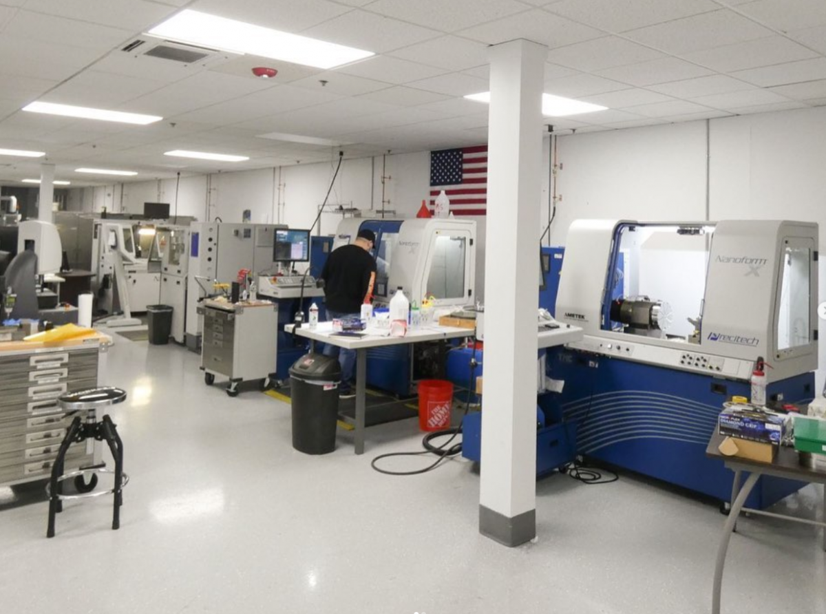
Spectral Systems’ Curved Optics Center of Excellence (COCE) has four diamond turning machines
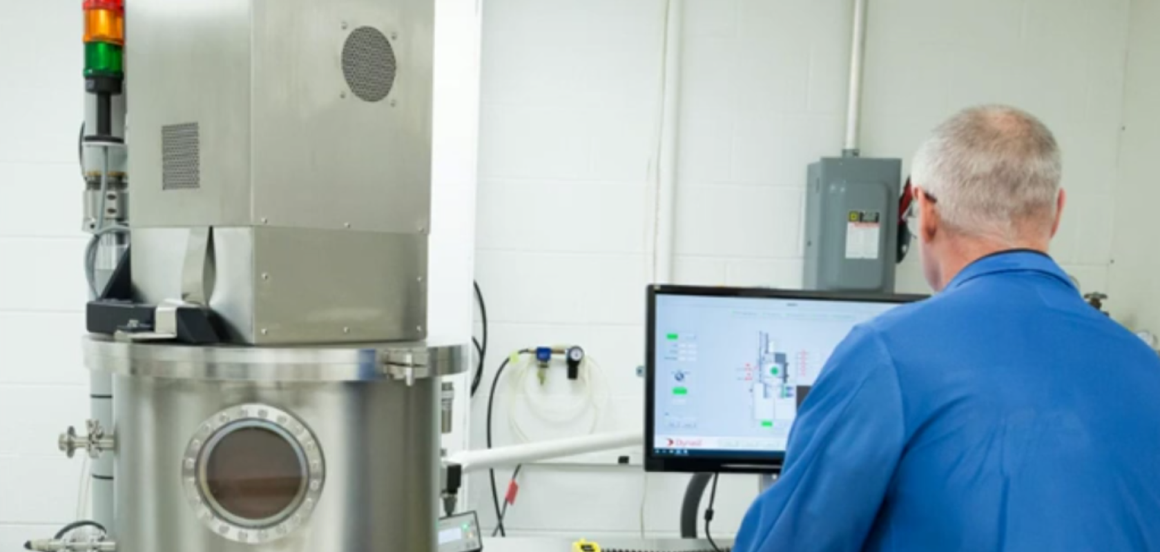
But even with a diamond turning technique perfected, like Spectral Systems has achieved via its Curved Optics Center of Excellence (COCE) with four diamond turning machines and a wealth of expert team members, the next stages of the supply chain can also throw up some challenges. Revealed Olsen: ‘Having a supplier that can apply diamond-like carbon (DLC) coating to chalcogenide materials is significant, because a lot of people don’t do that. I’ve been working with chalcogenides for the last 20 years and historically, applying diamond-like DLC coatings on chalcogenides, particularly if they don’t have germanium in their makeup, has caused a yield problem and we would get around 40 to 50 per cent yield. With innovative coating designs and deposition techniques we can now get up to 90 per cent yield.’
The reason for this is a strategic partnership with specialist coatings company, Evaporated Metal Films (EMF). The company has more than 80 years’ experience in thin film coatings, and has invested a great deal of time and effort in developing a coating system for producing long-lasting diamond like carbon (DLC) coatings on chalcogenides at scale.
Michelle Henderson, optical sales manager at EMF, explained: ‘About five years ago, we had an employee at our sister company who was very intimately involved with thin film coatings for coating IR materials. He suggested that this one chamber we had would be perfect for doing these types of coatings. So we built the business case and thought it was a good time for us to enter that space. We made some investments and revamped some chambers to be able to support the coatings that were needed. But the material that’s often difficult to coat is chalcogenide.’
Coating challenges
The main coating challenges when it comes to chalcogenides is non-uniformity, stresses, adhesion and pinholes. To overcome these, EMF designed its own DLC coating chamber based on a proprietary plasma enhanced chemical vapour deposition (PE-CVD) process, specifically for chalcogenides. Put simply, the system coats up, instead of down, with the substrate being coated suspended at the top, rather than sitting at the bottom where debris can settle. The cylindrical design allows the plasma cloud to be radially symmetric to the deposition plate, for a more uniform coating across the optic, and the chamber has an extra-large workspace to accommodate optics up to 14” in diameter, which can practically eliminate pinholes and minimise defects.
Another challenge with chalcogenides is the interface between the substrate and the DLC coating, which can often lack the necessary adhesion for practical use. Henderson explained: ‘It’s a challenging material to get the DLC to stick to because of the coefficient of thermal expansion (CTE) of the DLC, compared to the CTE of the substrate material. They have to match in order to get a good adhesion, and they don’t. The EMF secret sauce is in the pre-binder layer to get that DLC to stick.’
But the process doesn’t stop with fabrication and coating. The nature of chalcogenides means that there are many other factors to consider, as Henderson explained: ‘It’s not just about how it is fabricated or coated, but achieving real success will come from how the material is handled all the way through that process. For example, making sure it is properly stored while it is waiting to be diamond turned, and between the time it is finished diamond turning and the time it gets to us, in a low-moisture environment using desiccant packets to absorb the moisture, because chalcogenides can absorb some of that moisture, and then you can run into some issues with adhesion. Some of these things we had to learn by trial and error, going through and saying, “okay, we had an issue here, let’s walk through what the process was – beginning and end – what we know about the material,” to come up with the solution.’
Reference
“Near-Infrared to Ultra-Violet Frequency Conversion in Chalcogenide Metasurfaces.” Jiannan Gao, Maria Antonietta Vincenti, Jesse Frantz, Anthony Clabeau, Xingdu Qiao, Liang Feng, Michael Scalora, Natalia M. Litchinitser. Nature Communications, 2021. DOI: 10.1038/s41467-021-26094-1
Find out more about handling chalcogenides through the manufacturing and coating process by downloading the latest white paper.