The future of the global semiconductor industry
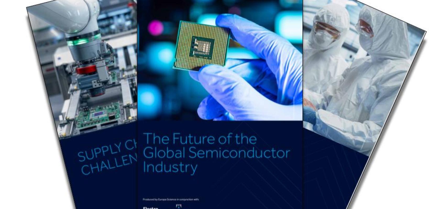
The future of the global semiconductor industry - A Materion Balzers Optics White Paper
How semiconductor leaders are navigating AI demand, supply chain pressure and next-generation manufacturing
Semiconductors sit at the heart of modern innovation — powering everything from AI infrastructure and hyperscale data centres to electric vehicles, healthcare systems and advanced communications networks.
But as global demand accelerates, semiconductor manufacturers face mounting pressure to improve performance, strengthen supply chains and scale production without compromising precision or profitability.
Produced by Electro Optics in conjunction with Materion, this expert-led report brings together insights from leading voices across automotive LiDAR, silicon photonics, sensing and autonomous vehicle engineering.
Inside the White Paper
Discover:
- The biggest supply chain and geopolitical challenges facing semiconductor manufacturers
- Why optical technologies are becoming critical for wafer-level metrology and lithography
- How AI growth is reshaping semiconductor infrastructure and investment priorities
- The role of co-packaged optics and photonic integrated circuits (PICs) in reducing power demands
- Why inline metrology and wafer-level accuracy are becoming essential for yield optimisation
- How semiconductor firms can overcome scaling, standardisation and production bottlenecks
- What manufacturers should look for in long-term supplier and co-development partnerships
Learn from leading semiconductor experts
Featuring perspectives from industry specialists including:
- CORNERSTONE, University of Southampton
- CSconnected
- Materion Balzers Optics
The report explores how manufacturers can maintain competitiveness while navigating increasingly complex production requirements, global supply chain risks and rapidly evolving customer demands.
Why this matters
The semiconductor industry is entering a new phase.
AI workloads are increasing power consumption dramatically. Manufacturing processes are becoming more specialised. Wafer-level measurements are shrinking to single-digit nanometres. And geopolitical pressures are forcing companies to rethink sourcing, production and resilience strategies.
This White Paper examines how semiconductor leaders are responding — from investing in optical innovation and inline metrology to building more collaborative, future-ready supply chains.
Key themes explored
Supply chain resilience
Learn why diversification, co-development and supplier alignment are becoming essential in an increasingly fragmented global market.
AI and optical innovation
Explore how photonics, co-packaged optics and edge AI are driving the next wave of semiconductor growth.
Wafer-level precision
Understand the growing importance of optical inspection, metrology and process feedback loops for improving yield and accuracy.
Manufacturing scalability
Discover how semiconductor firms can avoid production pitfalls while balancing cost, performance and innovation.
Who should download?
Ideal for:
- Semiconductor manufacturers
- Optical engineers
- Wafer fabrication specialists
- Photonics professionals
- Semiconductor equipment providers
- Supply chain and procurement leaders
- AI infrastructure specialists
- Semiconductor R&D and operations teams
Download the White Paper
Gain practical insight into the technologies, partnerships and manufacturing strategies shaping the next era of semiconductors.
Download now to explore how semiconductor leaders are preparing for the future of AI, photonics and advanced chip manufacturing.