
In June, fabless start-up Scintil Photonics shared that it had raised €13.5m (total raised to date: €17.5m) to help commercialise its silicon PICs with monolithically integrated lasers and optical amplifiers.
Scintil’s co-founder and CEO, Sylvie Menezo, talks to Electro Optics about the young company’s journey to date.
Congratulations on your recent second round funding success. Could you give a bit of background to the company?
I co-founded the company in November 2018, from CEA Leti, a world-leading research organisation in semiconductors. I had negotiated a licence to exploit a disruptive photonic integrated circuit technology, which consists of integrating lasers at the backside of advanced silicon photonics. This licence comprises about 20 patents and since our inception, we have also applied for 10 more patents.
Today, we are 15 people, 12 of whom are based in Grenoble, very close to Leti. Last year, we opened a subsidiary to hire three more people, and we plan to further grow this subsidiary.
Since our inception, we have been working with a very well known commercial foundry to prototype our circuits. We also have key partnerships for packaging our circuits and for developing control electronics for our circuits.
It was very important for us to have very early customers that take us from developmental projects to high volume production. So, we have three very nice leading-edge customers, which are leaders in the segments of high performance computing, 5G and data centres.
We have already shipped some prototypes to our customers, some of which have been tested successfully, and we are currently continuing to ship prototypes to other customers. So, it is highly motivating.
How were you able to form those relationships early on – with both the foundry and with your customers and partners?
With the commercial foundry, they liked the way we were – and are – integrating lasers, integrating lasers for optical communications is very key for the future. Now, in fact, we are focusing on short-reach applications. And the way to scale up in delivering high bandwidth high transmission rates is through parallelisation.
Today, what is being deployed is 400G, which requires four lasers, but 800G is coming in the next two years, and then 1,600G, 3,200G… and so on. As the bandwidth increases, you need to multiply the number of lasers. So it is very key to be able to integrate [lasers on the chip], otherwise packaging them starts to become very difficult, and very costly. Being able to integrate first of all allows you to have a lower cost, but it also allows you to perform with reduced optical loss and therefore at a higher – much higher – performance.
Laser integration enables parallelisation with higher performance, so you can scale to increase the data rate per wavelength, per lamba. So, we work on the two routes to be able to scale in bandwidth – parallelisation and higher bit rates – and we have demonstrated 100G per lamba. And we are also working on demonstrating 200G per lambda.
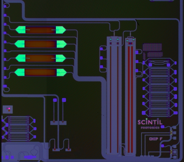
Scintil’s optical chip with integrated III-V optical amplifiers, supporting 1,600Gbit/sec data rate, enables the interconnection in high-speed communications. Credit: Scintil Photonics
This also drives lots of interest from the commercial foundry – they liked the way we integrate lasers relying on standard silicon photonics. This is key, not to require another completely different fab. So we stick to what's standard in terms of silicon photonics.
For packaging partners, these are people with whom I already had relationships with from my former network. I've been working in the field ever since I started working.
What kind of challenges do you see with commercialisation and how will you address these?
We want to be ready for mass production starting in 2024. So we need to scale wafer production from hundreds of devices to hundreds of thousands of devices. So there is the challenge of ramping up. We are happy to be working with a good commercial foundry, so ramping up in the volumes of the wafers, the circuits, we believe will not cause any challenges.
But then in parallel we have two types of customers, some of whom want standalone, photonic integrated circuits, but some want them to be packaged. So the other challenge is also to be able to ramp up the packaged device, which is necessary for industrialisation.
And, of course, reliability is very key in the application we are focusing on [telecomms]. So we also have to push reliability testing in volume. We've already had successful reliability tests that were performed by a French partner. But it is very key to assess that extensively, and this is what we will do over the next two years, along with having engineering prototypes running in the systems of our customers. So this is the challenge for industrialisation – ramping up and reliability.
And the other challenge is in commercialisation. There are minor customisations/add-ons we need to incorporate to allow our devices to be plugged into a customer’s system, but mostly we work on standards. And we need to deploy a commercial resource to enlarge our customers based on the same products we are developing.
How do you work with your customers?
We do prospection. We work on our next generation of chips and we demonstrate what we can do for potential customers. We ship the test, and, if they're happy, they want to go further.
We have nice projections for volumes, which I feel makes a big difference to locking in customers. Even though we work on next generation standards, and have a licence on a very good technology, we need to show that we can produce the next generation at high volume and low cost. So you have to show you can meet the cost targets, you can meet the performance and that you have set up a supply chain to be able to deliver in volume.
What are your thoughts on the European chips act and how it could benefit fabless start-ups in Europe?
To our knowledge, the process we are using to manufacture is not available in commercial foundries in Europe. So we had to go to the USA or Asia. I think if Europe could attract pure foundry players then there are lots of fabless start-ups like ourselves that would be ready to use them.
To attract foundries you need to have fabless companies. And I think in Europe we have a very, very interesting fabless scene. In addition to having foundries and fabless companies, there needs to be strong end users in Europe, which we have. So if there's a good trio like that, it can work with incentives from Europe.
How is the chips shortage affecting you?
The fab duration has increased, but it's acceptable for us. And the reason why is that we receive very strong support from our commercial fab. So it's very important that they are highly motivated, by what we are doing and the customers we have, which makes the impact, for now, okay for us. It's more on the electronic side on the components, you have to be very, very cautious. Currently, we don't buy really high volumes of electronic components, but we need to be very careful to be able to deliver at lower volumes for now and in the future in higher volumes.
Some types of components are getting really tough to get. We don't have huge volumes, so we can cope, but often you end up trying to find another component that works as an alternative as the one you wanted. I think this will be the case over the next two years.
We feel it on the electronic side for now. Photonics might also be more heavily affected in this way in the future but we are relieved that we get very nice support from our foundry with that.
What applications do you see in the future?
So our primary focus is optical communications, and more specifically, we want to support the deployment of HPC in the cloud. And so, these are very short-reach optical communications. Here the challenge is to connect large networks over large distances – that's why communications are required that have higher transmission rates over longer transmission lengths than standard electrical links.
First, it’s a really high growing market segment. At the centre of those short reach applications is data scientists needing to face the explosion of the data traffic while controlling the power consumption and the cost. 5G is the other segment – here our circuits enable the configurability of optics over existing infrastructure
What is key for these segments is the ability to to integrate lasers or optical amplifiers. And this enables them to scale in performance through parallelisation, or, because you have less loss or you can boost your optics, you can achieve higher performance.
So these are three segments that we focus on. But we also have some prospects in lidar applications and quantum. We also support some customer's prospects, when our standard circuits that we developed for optical transmissions can do the job for lidar or quantum we are very happy to sample in these side applications.
