
PIC innovation relies on having a supply chain that’s accessible – according to Victor Dolores Calzadilla, coordinator of the Open-Innovation Photonics pilot for North West Europe project
Photonic integrated circuits (PICs) are rapidly evolving into a more mature technology supported by an emerging but strong industrial ecosystem. In the coming decades, this technology is expected to have an impact in different sectors, such as transport, automation, health, communications, space exploration and many more.
Currently, most of the successful companies (vertically integrated) in the field are capable of design, fabrication and complete product development. This expensive way of operating has resulted in a limited number of consolidated companies, mainly in the areas that have large profit margins to justify the high investments, such as telecom and datacom. In order to lower development costs, widen the applications spectrum and unlock innovative SMEs, the PICs ecosystem is shifting towards a more horizontal model where open-access and open innovation are key. While several companies already provide open-access PIC technologies, open innovation in the field is still in its infancy.
In the open innovation model, partners with common interests collaborate closely (ideally in the same facilities) to solve technological challenges and develop technology together. Equipment manufacturers, process developers and foundries with complementary expertise work together to tackle the next challenges on the horizon in order to move the technology forward to the next node. Since multidisciplinary expertise and highly expensive infrastructure are required in the PICs industry, it is definitely an area where it makes sense to join synergies to achieve a cheaper and faster technology growth. Furthermore, a collaborative environment sets out better conditions for innovative SMEs to kick-start.
In this respect, a new European photonics project has started in Eindhoven last November. Twelve partners from north-western Europe are creating an open innovation pilot line that will contribute to upgrading key equipment and processes for InP PICs manufacturing to the next level. This should, in turn, have an impact in increasing the production yield, improve PICs performance and reduce the cost of new products. The facility is meant for shared use by European SMEs. The €14 million project is supported by the European Regional Development Fund and led by the Eindhoven University of Technology. The project has the purpose of increasing the maturity of PICs from a Technology Readiness Level (TRL) of four to seven.
The development of front-end equipment customised for InP PICs manufacturing will be carried out in cooperation with AIXTRON (Germany) and Oxford Instruments Nanotechnology Tools (United Kingdom) in the existing NanoLab@TU/e cleanroom at the Eindhoven University. SMART Photonics (Netherlands) will validate the front-end of the pilot line and manufacture a small series of PICs for SMEs through multi-project wafer runs to save costs.
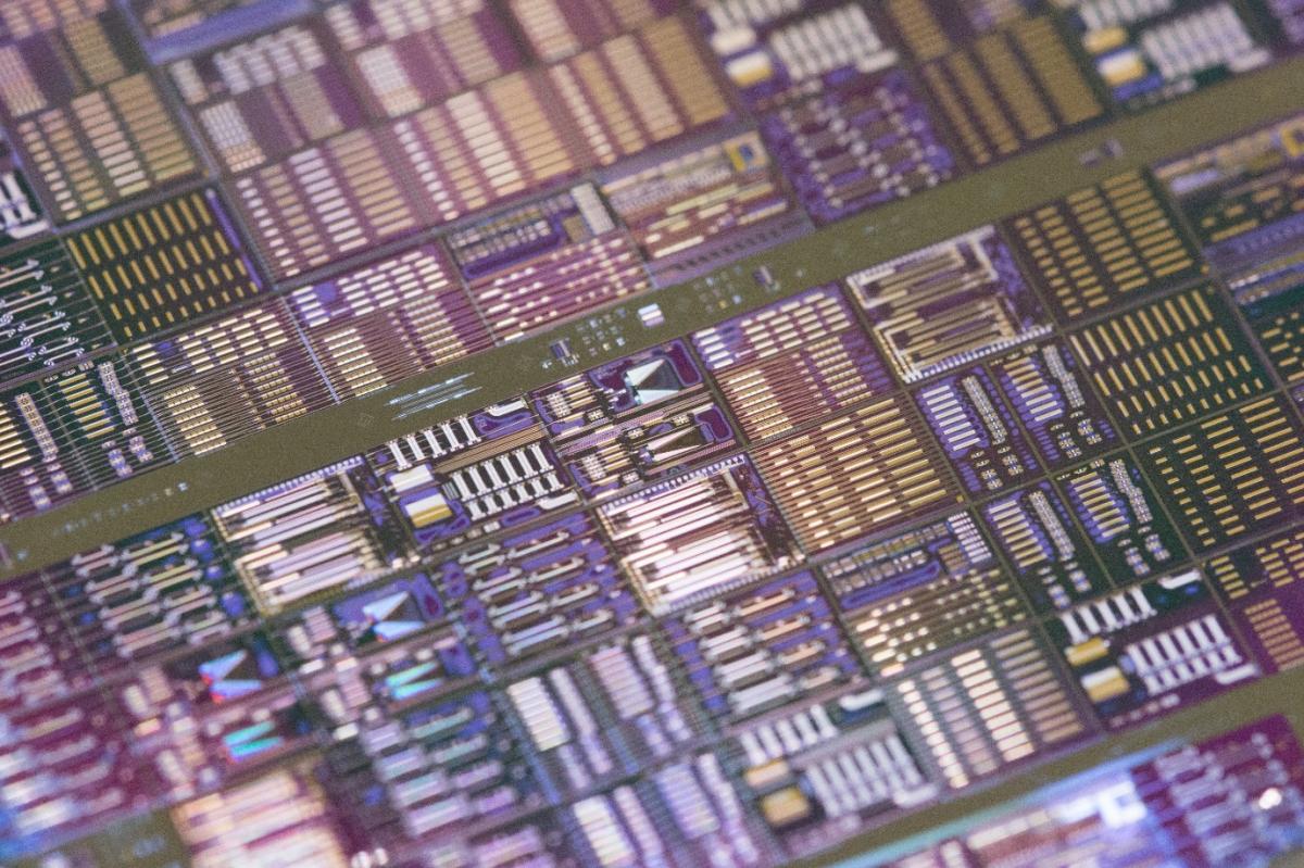
Examples of photonic integrated circuits. Credit: Florian Lemaitre
The back-end process will be done at the Vrije Universiteit Brussel (Belgium) and at the Tyndall National Institute (Ireland). Other parties involved are VTEC Lasers & Sensors, Technobis Fibre Technologies (both Netherlands), mBryonics (Ireland) along with the clusters Photonics Bretagne (France), Cluster NanoMikroWerkstoffePhotonik (Germany) and Photon Delta (Netherlands).
This project is unique in the sense that renowned semiconductor equipment companies are collaborating with photonic integrated circuits experts (in the same clean room) to develop customised equipment for PICs. Having equipment manufacturers, researchers and foundries working together is the cornerstone of the open innovation model that has the potential to accelerate the PICs technology growth.
The OIP4NWE project is complemented by the InPulse pilot line project also started recently, which democratises access to industrial prototyping and pre-production of high-performance InP PICs. The project builds on the pioneering work of the Joint European platform for Photonic Integration of Components and Circuits, which is already offering PIC prototyping services.
The open innovation character of OIP4NWE and the open-access focus of InPulse, both led by the Eindhoven University of Technology, are promising for shaping an even more attractive and sustainable European PICs ecosystem. Both projects are supported by the European Commission, the Photonics21 Public Private Partnership, and the PhotonDelta integrated photonics eco-system.