Having complete control over the transportation of waves is a key challenge essential for numerous applications.
In acoustics, the transportation of waves has enabled sensing, ultrasound and navigational applications. In the quantum regime, control over electron and spin transport has brought major advances in the operation of transistors, diodes, computers, smart phones and nanoelectronic devices.
Meanwhile, in photonics, it is the control of light that dictates the success of technologies in our field.
The transportation of light waves in both the classical and quantum domains has led to rapid advances in science and technology, such as precise microscopes, health and gravitational wave detectors, solar cells, quantum keys, optical memories and micro/nanoscale storage cavities.
Earlier this year, a team of researchers announced their discovery of achieving a new level of control over light entering photonic crystals. Their new method, described in Physical Review Letters, enables light to be tunably steered deep into such crystals, well beyond the ever-present Bragg length. They say their results have relevance to applications such as efficient miniature light sources and tiny on-chip lasers, robust qubits, and 3D photonic integrated circuits that shuttle information encoded as photons instead of electrical currents.
Bragging rights
In daily life we see how mirrors and reflectors control how light waves propagate from one place to another. While conventional mirrors such as those in bathrooms are made of metals that absorb a sizable fraction of the incident light, over the years scientists have found that certain nanostructures allow them to realise near-perfect mirrors. Such nanostructures, which consist of periodically ordered materials with a spacing of the order of the wavelength of light, are called photonic crystals. They attract considerable technological attention due to their novel functionalities.
Photonic crystals can be realised by etching nanopores – each with a diameter one-thousandth that of a human hair – in a periodic arrangement. Crystals can be tailor-made to perfectly reflect a chosen colour band, creating a ‘forbidden’ gap of light known as the photonic band gap. Light waves in the photonic band gap can only travel a limited distance through the crystal – known as the Bragg length (in honour of father-son Nobel Prize winning duo William H. and William L. Bragg) – before being reflected due to Bragg interference (see figure 1).
The photonic band gap was predicted in 1987 by American scientists Eli Yablonovitch and Sajeev John (following work in 1972 by Russian scientist Vladimir Bykov) and is rapidly being integrated into light sources and lasers, efficient solar cells and novel technologies, such as real ‘invisibility cloaks’.
If an atom emitting in a ‘forbidden’ wavelength is placed inside a crystal, it stops emitting and remains forever excited, as light with these colours cannot exist within the crystal.
This control on emission properties has led to a wide variety of additional applications, such as optical memory – storing information encoded as light – and nonlinear processors for quantum computing.
Exploiting imperfection
One of the main features of a photonic crystal is that once it has been fabricated, its properties are fixed, including the Bragg length. Recently, however, the team of scientists, from the University of Twente (Netherlands), the University of Iowa (USA) and the University of Copenhagen (Denmark), discovered a method to tunably steer light into photonic crystals to depths well beyond the Bragg length.
They achieved this by spatially shaping the incident light waves so that the energy density of the light is enhanced at tunable distances deep inside the crystals. The technique takes advantage of new wave forms that are induced by unavoidable fabrication deviations of the crystals’ nanostructures from their design.
The researchers first fabricated high-quality photonic crystals from silicon using semiconductor industry (CMOS) compatible methods, which make them suitable for on-chip integration. The crystals consist of tiny pores, each a thousand times thinner than a human hair, etched in silicon using an etch mask. The crystals exhibit excellent powerful gaps in the telecom wavelength range.
The team then directed unstructured plane waves onto the crystals. Using a camera, they viewed the light that leaks through the top surface, which represents the energy density of light at any given position inside the crystal. As expected for good quality crystals, the images revealed that light hardly penetrated into the crystal (see figure 2a), with 95 per cent of the incident light being reflected.
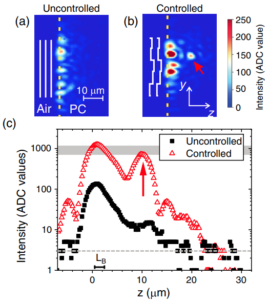
Figure 2: Steering of telecom light inside a silicon photonic crystal. The false colour camera images show that light incident with plane wave front (a) does not enter inside the crystal, while an intense spot marked by the red arrow (b) was observed at a depth of 10μm inside the crystal upon steering. The depth-dependent intensity of light inside the crystal extracted from the false colour images (c) shows a hundred-fold intensity enhancement with steering at the target location.
Next, the researchers chose an arbitrary position inside the crystal where light should be delivered. To this end, they shaped the incident wavefronts using a spatial light modulator – a central component of many projection devices. By programming the incident wavefront using the spatial light modulator, the authors realised a bright spot deep inside the crystal (indicated in figure 2b).
The authors observed a hundred-fold enhancement of light at the chosen location, which was five Bragg lengths deep. For comparison, if the incident light would not be shaped, the intensity at the chosen depth would
be severely decreased by a hundred to a thousand times.The technique takes advantage of the unintentional disorder (with tiny features less than a few nanometres) that occurs in all nanostructures. This small amount of disorder causes a small fraction of waves to randomly scatter into the crystal instead of being Bragg reflected. Therefore, by shaping the wavefronts of the incident light, the researchers ensure the light is selectively coupled into these wave channels that penetrate deep into the crystal. Moreover, by programming the wavefront correctly, these waves can be manipulated such that the intensity concentrates into a single location deep inside the crystal.
By being able to programmably steer the light, the researchers can direct it to any location within the crystal. Not only that, but by manipulating the wavefronts so that the light reaches multiple locations within the crystal simultaneously, this technique has the potential to improve the scalability of the aforementioned applications.
Practical opportunities
In explaining the practical benefits of this discovery to Electro Optics, Professor Willem Vos, of the MESA+ Institute for Nanotechnology at the University of Twente, used the novel analogy of a coffer: ‘Like a coffer, photonic crystals are fantastic for putting something inside and shielding it, for example, putting a packet of light inside a cavity,’ he said. ‘If you also put one or several quantum dots into this cavity, then you have a basic qubit, for instance, or even the basis of a laser or a nonlinear switch.’
Up until now though, while such elements could be stored within the crystal, they couldn’t be accessed. ‘The lid of the coffer remains closed due to the excellent shielding properties of the crystal,’ commented Vos.
However, with the researchers’ work now enabling light to reach much deeper inside the crystals, any functional elements previously stored within photonic crystals can now be accessed.
‘And at the same time, each of these functional elements is still profiting from the coffer aspect,’ continued Vos. ‘You could say we are providing the ability to peek into the coffer and flick a switch on the inside with your finger. Whereas previously your finger wouldn’t have gotten past the lid.’
Being able to access the inside of the crystal this way has applications in optical and quantum information processing, according to Vos, who explained that tiny pieces of photonic crystal could be used as switch or light-steering components in photonic integrated circuits. ‘Our method of wavefront shaping enables information inside these crystal [pieces] to be accessed with an incredible efficiency,’ he said.
Open for collaboration
With regards to developing technologies based on this research, Vos has no current intentions of doing so himself, but is very encouraging of other groups and companies putting this method to practical use.
‘I would be perfectly happy if other groups or even companies are interested in using this method to develop devices,’ he said. ‘We are happy to collaborate with industry. Right now, our current industrial partners are not focused on photonic integrated circuits. For example, our partners such as Signify – formerly Philips Lighting – the lithography firm ASML, Lumileds, Schott, mechatronics company Demcon, and TNO (a large Dutch company working in space optics), are currently more interested in wavefront shaping [technology] than in photonic crystals. So, if those in institutes who work on photonic integrated circuits want to pursue this in their work, I’d be very supportive of this and am very willing to help them onwards. We are open to a collaboration with industrial partners who come forward with an interest in putting this work to practical use.’
The research discussed here was supported by the NWO-FOM-programme ‘Stirring of light!’, STW-Perspectief programme ‘Free form scattering optics’, the MESA+ Institute section Applied Nanophotonics, the Center for Hybrid Quantum Networks (Hy-Q) at the Niels Bohr Institute, University of Copenhagen, and the P3 – Jumpstarting Tomorrow grant ‘UI-QSim’ by the University of Iowa.
For those interested in working with Professor Willem Vos, he can be reached at: w.l.vos@utwente.nl or by phone: +31 (0) 53 489 5388.