MEMs-tunable twisted crystal sensor from US universities enables optical power boost
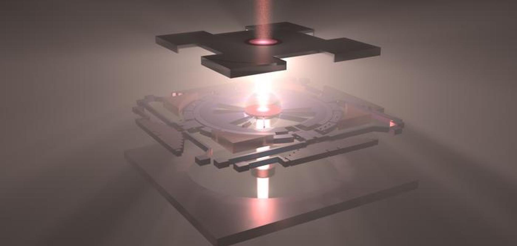
An on-chip twisted moiré photonic crystal sensor that uses MEMS technology to actively control the twist and distance between layers in real time (Image: Harvard SEAS)
Harvard, Stanford and UC Berkley collaborate on a MEMs-based optical sensor using twisted photonics crystals that they say could help to engineer smaller, more capable optical systems
Register for FREE to keep reading
Join 15,000+ photonics professionals staying ahead with:
- Exclusive insights, funding alerts & market trends
- Curated newsletters and digital editions
- Access to The Photonics100 list of R&D champions
- Exclusive panels & roundtables for professional development
- Technical White Papers & product updates to guide smarter decisions
Sign up now
Already a member? Log in here
Your data is protected under our privacy policy.