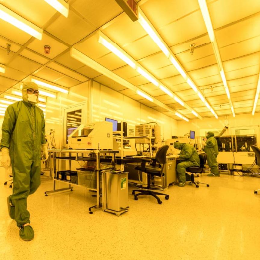
Advanced Micro Foundry (AMF), the world’s first silicon photonics specialty foundry has announced new multi-layer Silicon Nitride-on-Silicon (SiNon-Si) integration platform for Photonic Integrated Circuits (PIC). The new multilayer waveguide integration platform enables 3D photonic nanostructures to be densely integrated, resulting in compact footprint, low loss, higher device performance and fabrication tolerance.
Silicon photonics is a compelling and disruptive technology platform for realizing high performance semiconductor chips in emerging, as well as high growth markets such as data centers, telecoms, high performance computing, and consumer products. Generic silicon photonics are based on silicon-on-insulator (SOI) wafers, in which the photonic waveguides are formed in the topmost silicon layer, with integration of various functional devices, such as high-speed PN-diode modulator and Germanium photodetector which is monolithically grown on top of Silicon.
Based on such SOI platform, various silicon photonic products are developed, including optical transceivers, active optical cables, medical sensors, optical lidar, etc. “However, in some other products, such as very large scale (VLS) photonic integrated circuits, which requires densely integrated on-chip optical routing network, such SOI platform with only single waveguide layer becomes limited”, said Dr. Tan Yong Tsong, CEO of AMF. “Alternatively, additional waveguide layers with even lower optical loss is demanded in order to fulfil different complex requirements.”
In contrast to Si waveguide, SiN waveguide is with the merit of lower optical loss, which enables very large-scale waveguide routing network. Besides, SiN, due to the relatively low refractive index contrast to cladding oxide, also has large fabrication tolerance which is perfect platform for such as array-waveguide grating (AWG), etc. In order to address such application demand, AMF successfully developed multi-layered SiN-on-Si waveguide platform for three-dimensional (3D) photonic integration. With such platform, various silicon photonic devices including high speed modulators, Ge photodetectors, thermal tunable devices are integrated with additional SiN waveguides, to form either dual-layered SiN/Si or triple-layered SiN/SiN/Si waveguide system.

