Optical metrology cuts semiconductor fab waste at Fraunhofer IPMS
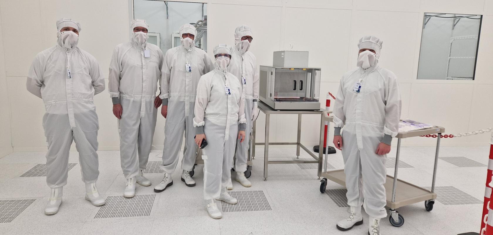
Experts from DIVE and Fraunhofer IPMS in the cleanroom at Fraunhofer IPMS in Dresden (Image: Fraunhofer IPMS)
Fraunhofer IPMS works with DIVE imaging systems to deploy a cleanroom-based, AI-powered hyperspectral wafer inspection system
Register for FREE to keep reading
Join 15,000+ photonics professionals staying ahead with:
- Exclusive insights, funding alerts & market trends
- Curated newsletters and digital editions
- Access to The Photonics100 list of R&D champions
- Exclusive panels & roundtables for professional development
- Technical White Papers & product updates to guide smarter decisions
Sign up now
Already a member? Log in here
Your data is protected under our privacy policy.