Skip to main content
Social media links EO
LinkedIn
Twitter
Log in
Register
Applications
Life sciences
Environment
Quantum
Defence
Automotive
Aerospace
Medical engineering
Electronics
Optical communication
Technologies
Illumination & energy
Imaging
Industrial lasers
Lasers & optoelectronics
Sensors, test & measurement
Photonics 100
UK Photonics
Photonics Frontiers
Resources
Webcasts
White Papers
Supplier
Events
Products
Search
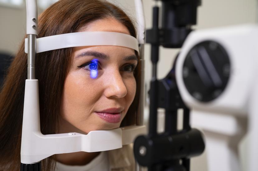
Quantum optical coherence tomography method developed for sharper retinal imaging
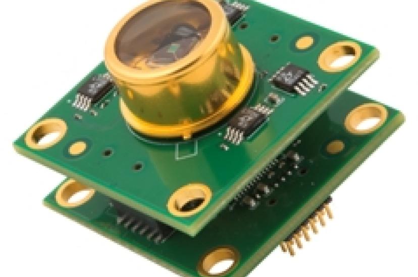
ICFO spin-off shinephi launches interferometric imaging method for semiconductor manufacturing
VTT brings silicon-on-insulator expertise to PIXEurope PIC pilot line
Photonics a “strategic asset” according to EU Tech Commissioner as sector urged to prepare for FP10
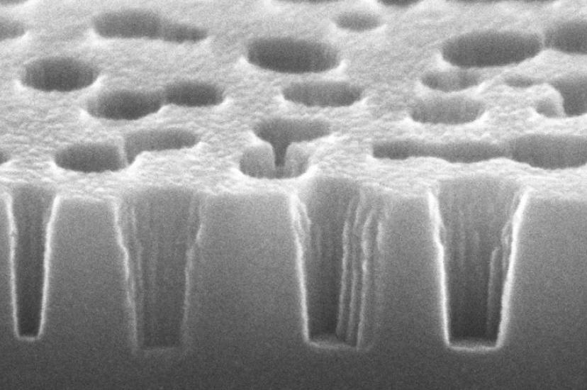
New way of fabricating anti-reflective glass avoids lithography
Graphene-CMOS integration on show at Photonics West
Media Partners