Skip to main content
Social media links EO
LinkedIn
Twitter
Log in
Register
Applications
Life sciences
Environment
Quantum
Defence
Automotive
Aerospace
Medical engineering
Electronics
Optical communication
Technologies
Illumination & energy
Imaging
Industrial lasers
Lasers & optoelectronics
Sensors, test & measurement
Photonics 100
UK Photonics
Photonics Frontiers
Resources
Webcasts
White Papers
Supplier
Events
Products
Search
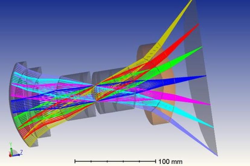
Ansys buys Zemax for optical modelling portfolio
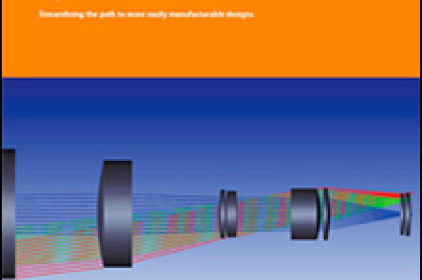
High-Yield Optimization - Streamlining the path to more easily manufacturable designs
LensMechanix
Small is beautiful
OpticStudio 18.7
Designing for Success
Zemax software now incorporates Edmund Optics product data
Media Partners