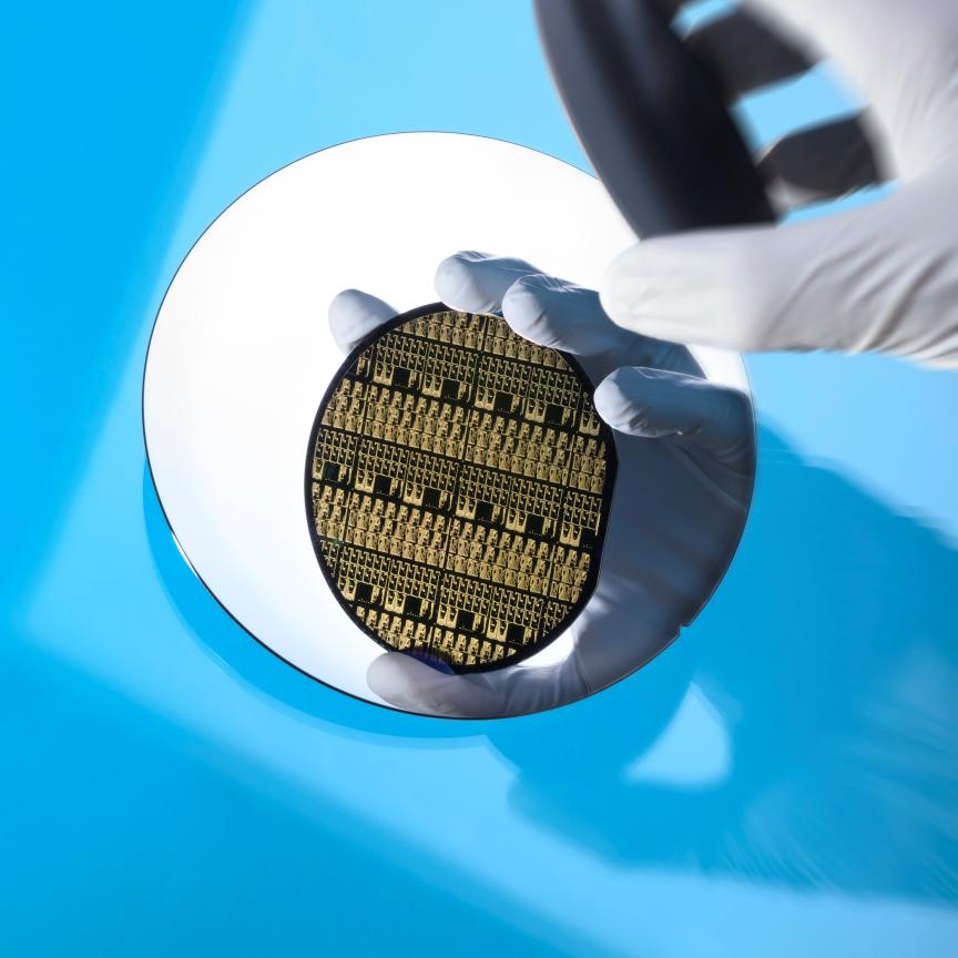
For Arlon Martin, silicon photonics has been a commercial reality since 2004. That’s when his then employer, Monterey Park, California’s Kotura, launched a silicon-based variable optical attenuator (VOA) into the telecoms market. ‘The VOA market is not huge, but we’ve grown to be the number one supplier and are shipping millions of units,’ said Martin, now senior director, marketing, at Mellanox Technologies following its acquisition of Kotura in 2013.
Building on lessons learned in VOAs, Mellanox today uses silicon photonics in much more important cable and transceiver roles. In these products, and those of several other companies around the world, silicon photonics is starting to fulfil its ample potential. While such offerings are largely limited to fibre-optic networking, other applications are now building on their progress. Diagnostics and intra-chip communications, for example, are exploiting an increasingly well-established body of knowledge in making use of silicon’s optical properties, and of the integration of germanium and semiconductor laser components. In doing so, they could take even greater advantage of silicon’s greatest promise: precision manufacturing on truly vast scales.
In transceivers, Mellanox is able to flip-chip bond indium phosphide (InP) lasers directly onto silicon chips, Martin explained. ‘We split the light using silicon photonics and that enables us to use a single laser for multiple channels,’ he said. ‘We then perform 25GHz modulation with a silicon on-chip modulator. When we do WDM, the multiplexer that combines multiple wavelengths onto a single lightwave pipe – which is then connected to the outside world – is also silicon.’
This approach makes Mellanox the only silicon photonics networking group that’s not using components like lenses, isolators or beam collimators, Martin said. The level of integration in the chip prevents dust entering and interfering with critical functions, so Mellanox doesn’t need expensive hermetic packaging. Using silicon for modulation also cuts the laser source’s price, Martin added. ‘We don’t need an expensive 25GHz laser that only has a couple of suppliers. We can just use a low-speed InP laser “lightbulb” that’s a 10th of the price.’
In March 2016, the company showed how silicon photonics will support future 200Gb/s networks, demonstrating its first key 50Gb/s modulator and detector building blocks. Key to obtaining the necessary speed is forming germanium waveguides, whose sizes are precisely controlled on silicon photonics chips. ‘We use the waveguide’s width to govern the speed,’ Martin said. ‘Most others use thickness. Thickness is a growth step, and it’s hard to control. But width is controlled by a semiconductor mask, which is extremely accurate.’
Such capabilities are converting communication component companies that weren’t originally interested in silicon photonics to the technology, with Martin citing the California-headquartered firms Finisar and Lumentum as examples. The Mellanox executive emphasises that the devices bring a cost advantage that he expects to become even more evident at higher data rates. Yet he admits that volumes are far from living up to the expectation created by some during silicon photonics’ early days of making ‘billions of these devices, like microprocessors’. ‘If you have that expectation, then silicon photonics is a failure,’ Martin conceded. ‘I would position it far differently in that the advantage of silicon photonics is that we don’t need the latest and greatest fab technologies. In our case we’re using eight-inch fabs.’
This ‘piggybacking’ of silicon photonics on an existing technology base is the key to its success to date, agrees Roel Baets from Ghent University (UGent) in Belgium. ‘The more you do that the more you profit from that advantage,’ he said. Baets has worked closely on silicon photonics with Belgian research institute Imec, including in founding the ePIXfab multiproject wafer service, recently taken over by Europractice. ‘As much as possible, people are trying to use the process set that’s standard in a CMOS fab, perhaps with a bit of tweaking,’ Baets stressed. ‘There are a few things that sometimes need an extra non-standard tool.’
Baets has seen what he describes as ‘a fairly steep growth curve’ in the industrial uptake of silicon photonics in recent years. He refers to Carlsbad, California’s Luxtera, which originally made silicon photonics at what was then Freescale Semiconductor’s Austin, Texas CMOS fab. Needing to move to a more advanced CMOS node, Luxtera is now collaborating with Geneva, Switzerland, headquartered silicon powerhouse STMicroelectronics, which has ‘invested heavily in silicon photonics manufacturing’. ‘That was one of the big triggers for STMicroelectronics, to develop an industrial platform, obviously not exclusively for Luxtera, but many industrial users,’ Baets observed.
Testing applications
Some of Baets’ research involves moving silicon photonics away from telecommunications, shifting wavelengths towards the visible and applications towards the medical. ‘As an example, we want to develop a very tiny coin-like device, which could easily be implanted under the skin of diabetes patients,’ Baets said. The devices will use light from an InP light source to the silicon to perform absorption spectroscopy on tissue fluids, staying in place for six months. They can be powered by wireless induction, continuously monitoring glucose level variations which Baets says ‘can be wild in diabetes patients’. The devices can also exchange data wirelessly.
By contrast, another young silicon photonic medical device company is avoiding the fully integrated approach common in optical networking. Cary Gunn, chief executive officer of Genalyte, based in San Diego, California, said that his company’s approach is the opposite of companies like Luxtera, which he also co-founded. Genalyte produces disposable silicon chips that carry 128 passive ring resonators, and the Maverick instruments that contain the active components to interrogate them remotely. ‘We kept the disposable piece’s cost as low as possible,’ Gunn said. ‘There are no active devices, just silicon and biology.’
The biological component is either an antibody or a protein attached to the chip that interacts with target material in the blood sample. The ring resonators trap a standing wave whose frequency shifts as the target material binds. ‘Our machine is taking a small drop of blood and looking at the frequency shift of all 128 sensors simultaneously, doing the tests in about 10 minutes,’ Gunn explained. To date, Genalyte has sold more than 20 instruments to research groups, principally for monitoring whether clinical trial participants are experiencing an immune system response to antibody drugs. They’re also now developing a larger number of diagnostics tests for use in everyday medical testing, although Gunn stressed that such use has not yet been cleared by regulatory agencies.
‘It’s all about finding a customer who’s going to use a lot of tests, as we make money on the chips,’ Gunn explained. ‘It’s a razor/razor blade business model. If you look at the number of diagnostic tests that are performed on a daily basis, it’s hundreds of millions just in the US.’ And if this kind of diagnostic use is taken up widely, it could begin to approach the impact that was originally foreseen for silicon photonics. ‘The silicon that would be consumed would be a major fraction of semiconductor industry volume,’ Gunn enthused. ‘I really think that this is the killer app for silicon photonics.’
Researchers at the University of Southampton, UK, are also developing silicon photonics technologies that could be used in chemical and biological sensing, for example detecting terrorist threats. They’re targeting longer infrared wavelengths, accessing the ‘fingerprint region’ in spectroscopy where characteristic absorption lines appear that identify particular chemical species.
‘Goran Mashanovic in my group is looking at how far we can push silicon-on-insulator (SOI),’ explained Southampton’s Graham Reed. A key problem in going to longer wavelengths is that light begins to move into the silicon dioxide cladding areas around silicon waveguides. To prevent this, Mashanovic controls the oxide region’s refractive index by selectively etching it away. His approach can support silicon photonics at wavelengths up to 3.8µm. However, the Southampton scientists are also working at wavelengths as long as 14µm, again by exploiting the capabilities of germanium.
Deployment everywhere?
Reed and his colleagues are also working on automated ‘passive alignment’, simplifying coupling both optical fibre and semiconductor lasers onto silicon photonics chips. While the Southampton researcher emphasises that this should lower costs further, he’s cautious not to overstate the importance of integrating lasers into silicon photonics. The classic case where people have argued this is necessary is ‘infra- and intra-chip communications’, which were originally seen as a driving force for silicon photonics, according to Reed.
‘Moore’s law is running out of steam and shrinking transistors is not necessarily the answer,’ Reed said. Part of the problem is that the interconnect that transfers data in and out electrically imposes a physical space limit on bandwidth, and is inefficient. Therefore, microprocessors that communicate optically rather than electrically might help computing sustain its traditional rate of advance. Yet Reed disagrees with the idea of putting lasers on microprocessors.
‘Interconnect isn’t the only limiting factor,’ Reed said. ‘Microprocessors run very hot, and a laser would be one of the most power hungry devices you could put on it. So, there’s a good debate to be had whether that laser should be put there. I don’t think it should. Data centres become a very different argument, because the laser’s not sitting on a microprocessor. You haven’t got the same thermal problem.’
Chen Sun, chief technology officer at Ayar Labs in Berkeley, California, added reliability as an argument against integrating lasers and microprocessors. ‘One of the primary modes of failure in an optical module comes from the short average time to failure of a laser,’ he said. ‘System makers remain scared of bringing optics deeper into the system. If you keep the laser separated, this opens up the possibility for keeping the lasers somewhere that is field-serviceable, while moving all other optics deeper into the system, a proposition that is very attractive to system makers.’
Sun has therefore used external lasers in his otherwise highly integrated silicon photonics work with University of California, Berkeley’s Vladimir Stojanovic. With their colleagues, they were able to produce individual silicon microprocessors combining more than 70 million transistors and 850 photonic components that provide logic, memory, and interconnect functions. And the most important element of their work is that the chip was made with a ‘zero-change process’ – that is, on an existing 45nm SOI manufacturing line, without any tweaks.
‘Our designs feature full photonic links with several key device components: grating couplers, spoked-ring modulators and silicon-germanium photodiodes,’ Stojanovic said. ‘Each of these uses the existing process technology to create a device and bypass its inherent constraints, and sometimes even create record-breaking devices – for example record vertical grating couplers. Zero-change process makes it far easier to combine multiple photonic links onto a single piece of silicon, offsetting laser and packaging costs and driving the overall $/Gb/s price down significantly.’
Ayar Labs is now working on using the approach that produced the microprocessor chips commercially. ‘We are currently putting together demonstrators that showcase the bandwidth density, power, form factor, and architectural advantages of the technology,’ said Sun. ‘We believe that the introduction of “just good enough” photonic components will enhance existing applications and enable a whole new range of cost-effective ones,’ added Stojanovic. ‘Adding photonic devices to CMOS chips opens doors to lots of other communication and sensing applications where tight integration, with lots of connections and high-sensitivity, are needed – such as lidar.’
That would be a step closer to what Reed would consider the ultimate success of silicon photonics: deployment everywhere. ‘If eventually you get massive bandwidth to your house it will come down a fibre and there will be a silicon photonics chip on the end,’ the Southampton researcher predicted. ‘There will be silicon photonics in every microprocessor, in every computer.’ He believes that it will take a large commitment to the technology from an industrial giant for that to happen.
And while Baets is less specific, he’s similarly optimistic about the prospects of silicon photonics. ‘Before 2005 it was an exotic research field,’ the UGent academic said. ‘Less than 10 years later, we have many major companies keeping a close eye on the technology or developing products. That’s remarkable. Give it another 10 years and it may become really big.’