
Coherent unveils module architecture for dynamic illumination and sensing
To address the rapidly growing demand for high-performance optoelectronic subassemblies that fit in consumer electronics for optical sensing applications, Coherent has unveiled a module architecture for ultracompact dynamic illumination and sensing with backside-emitting vertical-cavity surface-emitting laser (VCSEL) arrays.
The technology enables ultra-compact pattern projectors, flood illuminators, and tightly integrated sensing subsystems. It relies on an innovative flip-chip assembly of backside-emitting VCSEL arrays on application-specific integrated circuits (ASICs) and supports the integration of photodetector arrays.
“The flip-chip approach eliminates the parasitic inductance from bond wires, improving the depth resolution and accuracy of time-of-flight sensors in consumer electronics,” said Dr Julie Sheridan Eng, Coherent’s CTO. “Backside illumination optoelectronics enables not only the superior electrical performance of flip-chip assemblies, but also a higher level of optical integration with polarisation-locking and beam-shaping features embedded in the optoelectronic device.”
The VCSEL arrays can be designed to independently address individual or groups of emitters that are steered through diffractive optics, enabling the selective illumination of a region of interest within a dynamic scene.
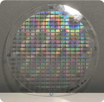
New CMOS area image sensor from Hamamatsu Photonics
Hamamatsu Photonics has introduced a new S16101 CMOS area image sensor.
Designed with a back-illuminated structure and a 1,280 x 1,024 Active Pixel Sensor (APS) matrix, the new sensor is ideal for applications not only in the visible spectrum, but also with spectral components in the ultra violet (UV) and near-infrared (NIR). Boasting high-UV sensitivity from 200nm, this non-cooled CMOS area image sensor delivers a spectral response to 1,100nm and is stable in UV light irradiation. Its sensitivity makes it ideal for industrial applications such as the detection of glues or resins in quality control.
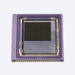
Due to the electronics integrated within the sensor, including the built-in timing and bias generators, amplifiers and A/D converters, the output signal is digital (LVDS). Additionally, the S16101 can reach a high-reading speed of 146 frames per second due to a reduction in the number of pixels along the vertical axis. It is also possible to reduce the number of vertical pixels to further increase the readout speed.
Finally, on top of offering the choice of rolling or global shutter readout, the new sensor utilises industry-standard SPI communication consisting of partial readout, gain switching, frame start mode selection functions, and more.
New spectrometer from IRsweep
IRsweep released its IRis-C spectrometer, which utilises dual-comb spectroscopy and quantum cascade laser frequency combs to offer high-resolution, high-speed sample analysis in a simplified, compact and cost-effective solution. The system delivers a combination of high stability, high optical power and high signal to noise ratio.
The spectrometer’s size and price make it ideal for a variety of settings in academic and industrial research. It also uses a modular approach, where the emission and detection units are separated, which further makes it suitable for integration into field applications ranging from stand-off detection to process monitoring.
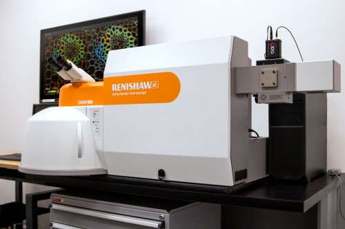
Renishaw introduces new functionality to inVia confocal Raman microscope
Renishaw has added fluorescence lifetime imaging microscopy (FLIM) functionality to its inVia confocal Raman microscope. In partnership with Becker & Hickl GmbH, experts in time-correlated single photon counting (TCSPC), the system combines both Raman and FLIM in a single instrument. This integration can overlay both FLIM and Raman images with pixel-to-pixel correlation, thus increasing understanding of samples across a range of applications.
FLIM and Raman microscopy are complementary methods for label-free imaging of biological cells and tissue sections. FLIM provides insight into molecular interactions and can be performed at least 10× faster than Raman imaging. Meanwhile, Raman spectroscopy boasts high chemical specificity and high-resolution chemical images. The combination of techniques is therefore ideal for rapid identification of regions of interest by FLIM, followed by chemical and structural characterisation by Raman imaging.
For FLIM data analysis, comprehensive software from Becker & Hickl is included with multi-exponential, incomplete and shifted-component analysis models. The software also includes proprietary phasor analysis to distinguish lifetime populations. Fluorescence lifetime and Raman images can be directly overlaid due to the use of the highly accurate Renishaw MS30 high speed encoded stage for both imaging modalities.
Wenglor presents new triangulation laser distance sensors
Wenglor has its new P3 series of triangulation laser distance sensors, which offer precise measurement results at distances of up to 1,000mm – accurate to a few microns.
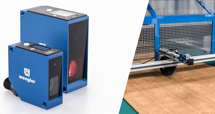
The 32 sensors of the P3 series are offered in high-quality aluminium housing with built-in ‘TripleA’ technology – Aspheric Dual Lens, Adaptive Auto-Exposure and Active Temperature Control.
- Aspheric Dual Lens: Two specially shaped aspherical lenses, ensures improved image quality of the laser light spot and thus increases optical precision.
- Adaptive Auto Exposure: Enables the exposure time of the CMOS chip to be adjusted automatically. This makes it possible to expose both bright and dark objects, regardless of the material, to achieve good results.
- Active Temperature Control: ensures temperature-stable operation. Several temperature sensors built into the housing continuously measure the internal temperature. The benefits: The warm-up time of CMOS sensors is significantly shorter compared to other sensors of this type.
The P3 series comprises 32 models in total, divided into five measuring ranges for small and large distances from 30mm to 1,000mm. The high-quality aluminium housing, the glass lenses protected by a PMMA disc and the built-in temperature sensors ensure high temperature stability and short warm-up phases. P3 sensors can be supplied with either red or blue laser light, and are also available as digital or analogue versions. The digital models can be configured directly via teach-in, the analogue models via OLED display or via an integrated Bluetooth interface.
The IO-Link 1.1 communication standard with the highest transmission speed COM3 also enables measurement data to be read out quickly. The power of the laser can even be changed to adapt the sensor to individual requirements: The P3 sensors are supplied in laser class 1 and can be switched to laser class 2 via a licence.
New air bearing stages from PI USA
Physik Instrumente (PI) USA, has launched the PIglide A-123 family of wide-body, high accuracy linear stages. The low-profile precision positioning stages are equipped with preloaded air bearings, integrated linear encoders, and utilise cogging-free, direct-drive linear motors. The combination of these noncontact components produces a motion platform that operates without friction, delivering exceptional performance, quality, and longevity.
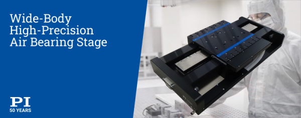
Air bearing stages are used in precision engineering, test and manufacturing applications in fields such as photonics, metrology and precision scanning in semiconductor or flat panel display manufacturing, where extremely precise and accurate movement is required.
Thanks to a high-force linear motor, the linear translation stage can reach peak velocity in milliseconds, while the high-capacity air bearings can support payloads of up to 60kg (130lbs). The A-123 series features a laterally opposed bearing design, with actively preloaded air bearings that allow for mounting in any orientation. It is available with travel ranges from 50mm to 750mm, can achieve 30m/s² acceleration, and reach a maximum velocity of 1,000mm/s. Stages are available with optional absolute encoders with 1nm sensor resolution and can achieve bidirectional repeatability of 0.1µm and calibrated position accuracy of 0.3µm.
PHABULOuS Pilot Line presents the first use cases
After two years of a collaborative effort involving multiple companies and research centers throughout Europe, the PHABULOuS Pilot Line for free-form micro-optical components presented its first use cases – for companies such as Seisenbacher, Swarovski, Forvia and Microoled – at OFC 2023 in San Diego, California, this month.
Seisenbacher, a global provider of interior solutions for the railway industry, is using PHABULOuS services to develop ultrathin luminaires and luminaires with a significantly reduced number of LEDs, with a customised shape of the illumination pattern. The image below shows the design of the freeform structure used per light source, realising a very homogeneous irradiance on the diffuser plane. The integration into the Seisenbacher luminaires has been finished and a comprehensive type test campaign is ongoing to prove the compliance of the final product with the harsh environmental conditions on railway rolling stock applications.
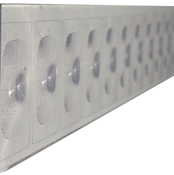
Replica of FMLAs imprinted onto a substrate using UV-imprint R2P (roll-to-plate) technology.
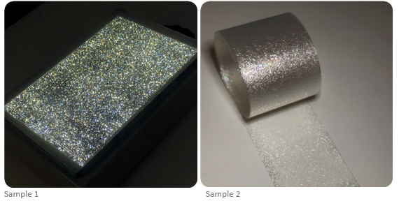
Swarovski, world leading manufacturer of luxury crystal components, is using the large-area roll-to-roll (R2R) and roll-to-plate (R2P) replication technologies offered by PHABULOuS to create micro-structured foils and panels with gemstone appearance. In Sample 1 below, we can see a lightbox that uses a freeform micro-structure on the luminaire to create a sparkling effect by imitating crystal facet structures. Sample 2 is a foil with a double sided structure that creates a sparkling effect.
Forvia, one of the larger automotive suppliers worldwide, is using the pilot line services to miniaturise optical systems for headlamp applications that will reduce installation space and weight while enabling low-cost manufacturing. The first results prove the potential of the freeform micro-optics, although some adaptions are still necessary to fulfill all requirements of the automotive market. In the picture below, we can see a double-sided optical component created using a Fresnel structure for pre-forming the light on the light entrance side, and a freeform facet structure on the light output side.
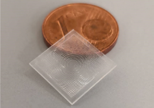
As small as a one-cent coin – and even thinner: a double-sided optical component created using a Fresnel structure
Microoled produces near-eye AMOLED displays and modules for a wide range of products, including high-brightness ultra-low-power microdisplays for light AR eyewear products. The firm was looking to control the angular shape of light output and enhance the brightness of its OLED micro-display components, especially in connection with compact, free-space optics-based micro-projection systems for wearable AR applications. The company is evaluating the performance and manufacturability of different designs of micro-optical elements in order to choose the right manufacturing process for industrialising the technology.
A replica of the free-form microlens array (FMLA) that will be assembled on top of Microoled's OLED microdisplay chips
Princeton Infrared Technologies selected by AFRL to develop 2.1µm wavelength cutoff SWIR avalanche photodiode
Princeton Infrared Technologies, a manufacturer of both shortwave infrared (SWIR) cameras and one- and two-dimensional imaging arrays, has been selected by the US Air Force Research Laboratory (AFRL) for a SBIR Phase II contract. The contract, in the amount of $749,907, targets the development of a small pitch Type 2 Strained Layer Superlattice (T2SLS) Avalanche Photodiode (APD) Focal Plane Array Multifunction LADAR Receiver. AFRL is looking to investigate the technology’s potential for filling capability gaps in the Department of the Air Force (DAF). The imager will be optimised for detection in the extended SWIR band, up to 2.1µm.
QKISS project developing ready-to-deploy European Quantum Key Distribution (QKD) systems
Launched in January, the QKISS (Quantum Key Industrial SystemS) project is a collaboration between two high-tech industrial groups, Exail and Thales, and two academic teams from Université Paris-Saclay and Sorbonne Université. Funded by the European Commission under the Digital Europe programme, the project aims to produce high-performance, secure, and certifiable European Quantum Key Distribution (QKD) systems within 2-3 years. QKD systems use the fundamental laws of physics to protect encrypted communications, making them highly secure.
QKISS will implement a complete and qualified telecom link for encrypted communications that will be compatible with existing telecom network systems. The project will include the manufacturing of opto-electronic components, the development of specialised signal processing and coding algorithms, and full system integration and field demonstrations. QKISS will also ensure that the QKD systems function together with Thales' Mistral encryptors, a turnkey network encryption system.
To ensure certifiability and compliance with EU standards, the design strategy will include limitations of attack surface, in-depth defense, and common criteria evaluations for the protection profile. The project will also feature a low number of external interfaces, a limited number of components for realistic system construction, an industrial architecture for legacy networks, and use of QKD as an add-on to existing IT needs.
QKISS targets a low-cost and high-rate implementation suitable for metro use-cases with very high speed of communication, with modulation rate in hundreds of megabaud (MBd) and secure key rate in megabits per second (Mbit/s). After an industrialisation phase, QKISS systems will be available for deployment in the EuroQCI and applications relying on private communications such as e-banking, e-health, government communication, or the management and protection of critical infrastructure.
Tower Semiconductor announces heterogeneous integration of quantum dot lasers on popular silicon photonics foundry platform PH18
Tower Semiconductor and Quintessent have collaborated to announce the world's first heterogeneous integration of GaAs quantum dot lasers and a foundry silicon photonics platform (PH18DB). This new platform will offer GaAs-based quantum dot lasers and a semiconductor optical amplifier (SOA) built on Tower's high-volume base PH18M silicon photonics foundry technology, which includes low-loss waveguides, photodetectors, and modulators heterogeneously integrated on a single silicon chip. This will enable dense photonic integrated circuits (PICs) that can support higher-channel counts in a small form factor for optical transceiver modules in data centres, telecom networks, and emerging applications in artificial intelligence, machine learning, lidar, and other sensors. The PH18DB platform complements Tower's previously announced PH18DA platform that offers heterogeneously integrated InP lasers, modulators, and detectors.
The open foundry availability of this 220nm SOI platform will provide access to a broad array of product development teams to simplify their PIC design through the use of laser and SOA pcells. Initial process design kits (PDKs) for PH18DB have been made available in partnership with DARPA under the Lasers for Universal Microscale Optical Systems (LUMOS) programme, which aims to bring high-performance lasers to advanced photonics platforms for commercial and defence applications.
Valeo announces two major contracts for its 3rd-gen lidar system
Valeo announced that its SCALA 3 lidar has been chosen by a leading Asian manufacturer and a leading American robotaxi company, with registered orders of the technology now amounting to over €1 billion.
SCALA 3 expands the domain of operation of conditionally automated vehicles (level 3) to wider areas and higher speed (up to 130kph), and makes robotaxi (level 4) deployment at scale possible. Boasting more than 12 million pixels per second and a detection range of 200m for low reflectivity objects and 300m for high reflectivity objects, it sees almost everything, especially objects that are invisible to the human eye. SCALA 3 also comes with a suite of software modules, including perception and AI-based algorithms, which can easily be embedded on major SoC platforms and run on dedicated ECUs or domain controllers.
Can't see your company's latest announcement? It may have already been featured in our latest product section earlier this month. If not, make sure we are receiving your latest technology updates at editor.electro@europascience.com.