Silicon photonics, or, more generally, integrated optics, is about implementing optical system components on a chip rather than in a classical way. One of the main drivers behind this technology development is miniaturisation, as integrated optics can provide a compact alternative for the bulky classical optical counterparts – including, for example, lenses, mirrors and light detectors. A second driver is the ability to create enhanced functionality and performance at a much lower price, and hence to take optical systems towards commodity level.
Integrated optics finds its origin in the 1960s, but has long remained an academic field of research. Roel Baets explained: ‘I see two reasons for this slow evolution. First, the research domain of integrated optics was much smaller than microelectronics, for example, explaining the lower investments. Second, researchers worldwide explored a wide variety of photonic technology platforms, slowing down the evolution towards industrial deployment.’
Silicon photonics technology and CMOS infrastructure: a fruitful marriage
All of this changed about 20 years ago with the idea of re-using the silicon (Si)-based technology platforms that were commonplace in the microelectronics industry. ‘On the one hand, using Si as the basis material for integrated photonics was a controversial idea, as Si is not the most suited material for realising optical functionalities,’ said Baets.
But on the other hand, the ability to re-use the technology maturity and existing infrastructure of the CMOS fab could largely boost the development of integrated photonics technologies.
That was also how Ghent University started developing Si photonics technology – first by focusing on passive components such as waveguides, later by developing active components, for example, that could modulate and detect light in Si.
‘Being associated to imec, we could make use of its advanced CMOS infrastructure and work closely with technology groups in Leuven.’
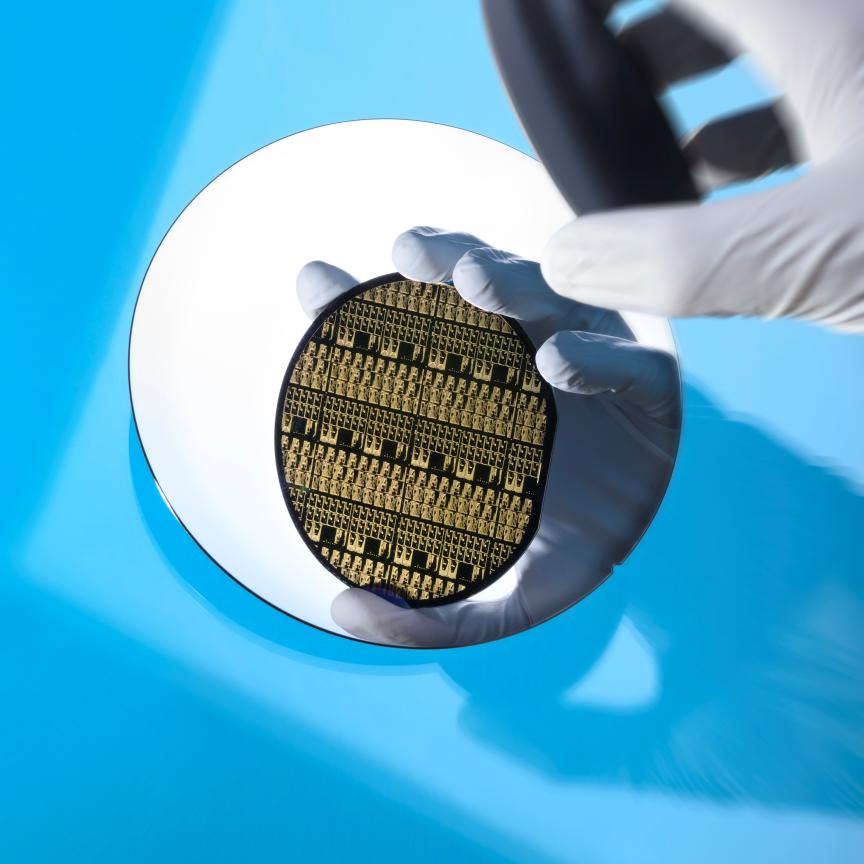
A silicon photonics wafer
From telecom to sensing
Silicon photonics was originally developed for fibre optic tele- and datacom applications. At both ends of a telecommunication optical fibre, you find optical transceivers that modulate and convert optical signals into electronic signals and vice versa, at a very high speed. Technologies are being developed for optical communication over long distances – with fibres spanning hundreds of kilometres – and over short distances, for example to interconnect the various server racks within a datacentre. For these applications, the main material platform for implementing optical functions is silicon on insulator (SOI), as it allows the propagation of light with wavelengths in the 1 to 2µm range – the same wavelengths that are being used in glass optical fibres.
About 10 years ago, people started to realise that the same chip technology could have an enormous potential for diverse sensing applications. A well-known example is lidar, which is being developed for robotics and autonomous driving applications. Si photonics has also found its way into structural health monitoring. In this application, fibre Bragg gratings are deployed to control the mechanical integrity of building-critical constructions. And finally, Si photonics holds tremendous promises for molecular analysis, for either gas detection or medical applications.
‘In years to come, I expect that the market volume potential of Si photonics for sensing applications might surpass the potential that the technology holds for tele- and datacom,’ noted Baets. ‘Think about the possibility of integrating small CO or CO2 sensors in everyone’s smartphone, or of creating an implantable glucose sensor that can regularly check a diabetic patient’s blood glucose level.’
The ability to produce Si photonics chips on large wafers and in large volumes largely supports this vision.
Sensing applications often operate with light in the visible or mid-infrared (mid-IR) wavelength range. As these wavelengths are not compatible with the standard Si photonics platform, different material platforms have been developed such as the silicon nitride (SiNx, or SiN for short) waveguide platform. Just like with silicon these new platforms are very compatible with the CMOS manufacturing infrastructure.
An integrated light source: The Holy Grail of Si photonics
Through the years, the material platforms for Si photonics have evolved into mature vehicles. However, a common challenge for these platforms is the lack of an integrated light source. Direct light emission from Si or SiN is highly inefficient. Therefore, today, the light source is being assembled as an external component. This component is made of III-V semiconductors such as indium-phosphide (InP) or gallium-arsenide (GaAs) – depending on the required wavelength range.
‘Worldwide, researchers are exploring a range of technologies to enable the integration of III-V-based light sources at wafer level,’ said Baets. ‘At imec/UGent’s Photonics Research Group, we focus strongly on micro-transfer-printing of the III-V-based devices. With this technique, III-V-based laser diodes are processed on a III/V semiconductor wafer and subsequently transferred and printed onto a larger Si wafer (200mm or 300mm). The almost-finished coupons are not transferred individually, but in large numbers, ensuring a highly scalable and manufacturable solution. This III-V-on-Si(N) is now gradually evolving into a third material platform for Si photonics, next to the SOI- and SiN-based platforms.’
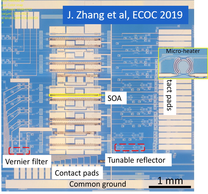
A III-V on silicon widely tuneable laser array for the telecom C-band, as reported at ECOC 2019
Access to SiP technology
Si photonics has become a success story, largely thanks to the ability of re-using the maturity of the microelectronics technology. However, the technology has not always been accessible to the photonics researchers.
Roel Baets explained: ‘When we started to research Si photonics technology, we were lucky to rely on the CMOS infrastructure available at imec. But many research groups worldwide – academic and industrial – did not have easy access to such a Si microelectronics fab. And this presented a huge challenge for the Si photonics research community, hindering researchers to turn their ideas into reality.
‘Gradually, we found a solution for this problem. In 2004, thanks to European funding, we were able to set up a Network of Excellence – called ePIXnet – that gathered the main European stakeholders in the field of integrated photonics.’ Baets continued. ‘Two years later, this network resulted in ePIXfab, which became the globally first multi-project-wafer (MPW) brokerage for Si photonics.
‘Research groups worldwide could now submit their designs, which are then combined onto one mask set. Wafers are collectively processed at shared costs, in either imec (Belgium) or LETI (France), by using the institute’s respective Si photonics platforms,’ he said.
For this foundry model – amongst other things – Roel Baets has been named the 2020 John Tyndall Award recipient.
Several years after being founded, the activities of ePIXfab were handed over to Europractice, a European consortium brokering MPW-services, originally for the microelectronics industry and academia. At imec, Europractice is operated by imec.IC-link. Today, it offers several MPW runs per year for Si photonics research and prototyping. The process flows run at research institutes such as imec and Leti. In 2020, Europractice will offer four MPW runs on imec’s SOI-based platform (called iSiPP50G), and two on imec’s SiN photonics platform, called BioPIX. Meanwhile ePIXfab has re-invented its role into being the European Silicon Photonics Alliance, largely with a mission of training and advocacy.
Same problem for industrial manufacturing
However, the challenge originally faced by the Si photonics research community is now repeating itself for industrial manufacturing. Baets said: ‘To move Si photonics beyond research and prototyping, mature Si photonics platforms need to run in true industrial fabs, ensuring high performance and fast turn-around-times. And this is an urgent challenge that is now mainly faced by smaller fabless actors within the Si photonics community.
‘In order to make this possible, industrial fabs need to invest in tools and establish mature process flows, to finally enable small- and high-volume production of Si photonics circuits. I expect that this will happen in the coming years,’ noted Baets.
First steps in that direction are being taken. Imec, for example, besides prototyping and low-volume production, has enabled a manufacturing route – together with a commercial foundry partner – to support higher volume demands. Interestingly, even the MPW fabrication modality is gradually moving to industrial fabs, a trend akin to what has happened in microelectronics.
European pilot lines
The fact that there are now two additional MPW runs on imec’s SiN platform was partly made possible by PIX4life. PIX4life is a European pilot line that was set up with a Horizon 2020 (H2020) grant. The goal of pilot lines for Si photonics is twofold: (1) carry out research and (2) increase the technology readiness level and set up the required infrastructure that can bridge the gap between research and industrial production. The project is being coordinated by imec’s Life Science Department.
Roel Baets said: ‘PIX4life was based on two SiN material platforms, each targeting different applications: the SiN BioPIX platform from imec and the SiN platform from Lionix, The Netherlands. It was conceived as the first open access pilot line for photonic integrated circuits in the visible range. It enables many different applications in the fields of biophotonics and life sciences, in which light is utilised as sensing mechanism or as instrument. Examples aremulticolour sources for spectroscopy or cytometry, optical coherence tomography (OCT) and labelled sensors.’
Meanwhile, other European pilot lines have emerged, where imec is largely involved. These include (1) PIXAPP, co-ordinated by Tyndall National Institute and focusing on assembly and packaging of photonic integrated circuits, and (2) MedPhab, a recently launched pilot line coordinated by VTT (Finland) and focusing on photonics technologies for medical applications.
The key remit of pilot lines is to become sustainable after the initial four-year duration and continue to offer their state-of-the-art technologies and services to potential users, in particular European SMEs.
--
Roel Baets is a full professor at Ghent University where he leads the Photonics Research Group, a mixed UGent – imec team. He received MSc degrees from Ghent University and from Stanford University, and a PhD degree from Ghent University. He has also held part-time faculty positions both at Delft and at Eindhoven University of Technology. For more than 35 years Roel Baets has worked in the field of integrated photonics, in multiple material platforms (silicon, silicon nitride, III-V). He is a Fellow of IEEE, OSA and EOS.
--
Further information
-
Visit the Europractice website to learn more about the MPW prototyping services for Si photonics at imec.
-
Read the press release and imec magazine article on Si photonics for next-generation datacenter interconnects.
-
The 2020 John Tyndall Award will be presented to Roel Baets at OFC 2020. More information via this link.
Roel Baets recently was named the 2020 John Tyndall Award recipient for 'seminal research in silicon photonics and for driving the foundry model in this field [silicon photonics]'.
John Tyndall was a 19th century Irish physicist who demonstrated the principle of total internal light reflection.
Total internal reflection is the basis of glass fibre optic telecommunication – allowing light to be transported through the fibre towards its end point, in principle without loss. Light transportation on a chip essentially uses the same principle. The main difference between glass fibres and silicon waveguides is the much smaller dimension of the waveguides on the chip along with a much larger difference in refractive index between the core and cladding of the waveguide structure – referred to as high index contrast.
Baets explained: ‘At the end of the 1990’s, we [Photonics Research Group] started exploring this high index contrast, because we realised that it would allow us to demonstrate new and vastly miniaturised optical functions, previously impossible. Soon we discovered that we would need a very high geometrical accuracy (nm-level) for making the waveguide structures,’ he said.
‘There is only one technology in the world that can guarantee such an accuracy, and that is CMOS technology. In addition, Si, having a refractive index of 3.5, can deliver such high index contrast when combined with a SiO2 (n=1.5) cladding,’ Baets continued. ‘For us, this idea was in fact the primary (and mostly scientific) reason why we started making use of the CMOS infrastructure at imec. A few years later, it became clear that this approach would potentially form the basis of new applications, new products and an entirely new industrial ecosystem.’

Grating couplers on a silicon-on-insulator platform, taking advantage of high-index contrast
From a scientific point of view, the principle of total internal reflection, demonstrated by John Tyndall, was used by Baets and his team to pioneer one of the key components of today’s photonic integrated circuits: the grating coupler. This component allows to connect photonic integrated circuits with the outside world.
Baets added: ‘By exploiting high index contrast, our team could establish an efficient coupling between the glass fibre and the waveguide structure on chip. This grating coupler – which can be considered the optical equivalent of the electrical wire bonds – is a crucial ingredient of today’s photonic integrated circuits and has also allowed their testing at wafer level.’