Efforts to make optical devices smaller, more integrated, and better able to exploit silicon manufacturing technology bring many advantages, but also create new challenges in managing the heat they experience. Designers must therefore think hard about removing this heat, in particular within photonic integrated circuits (PICs).
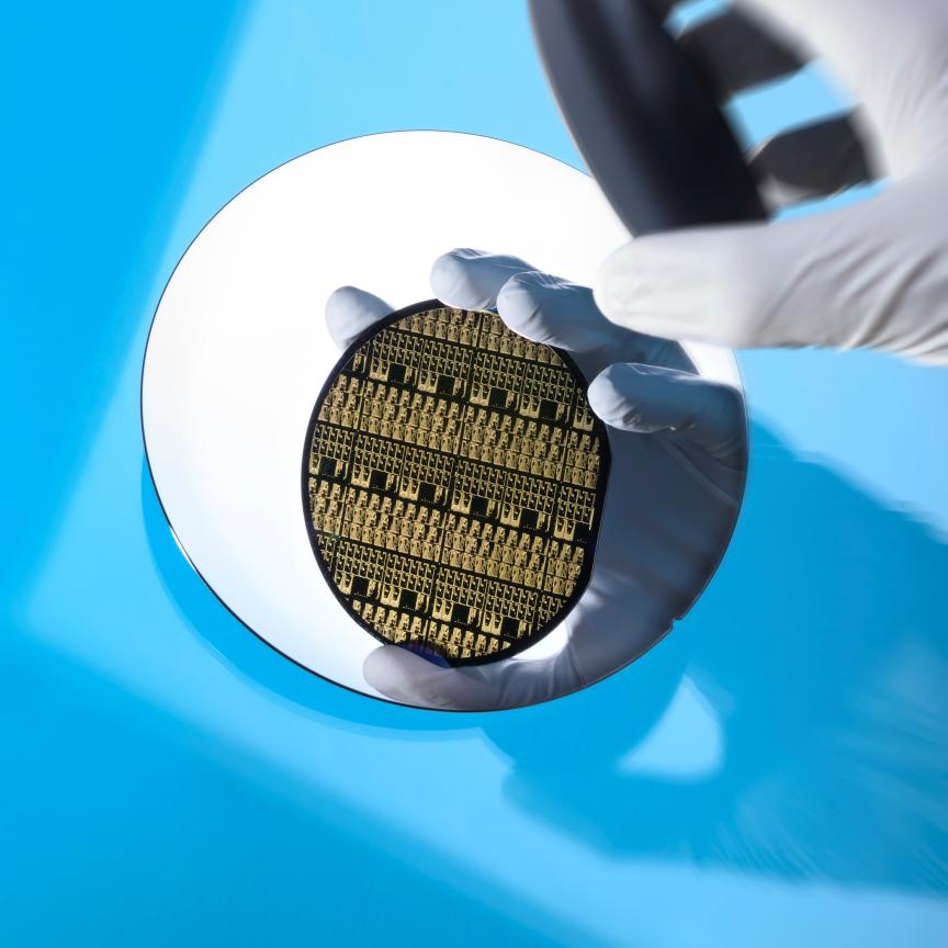
One key integration driver has been silicon photonics, bringing higher yield and lower chip cost by effectively pre-assembling photonic circuits using lithography. Quentin Wilmart is a researcher from Leti in Grenoble, France, working on this opportunity in the European project CmOs Solutions for Mid-board Integrated transceivers with breakthrough Connectivity at ultra-low Cost (COSMICC). It aims to develop economical integrated optical transceivers based on silicon photonics for data centres. ‘Our approach is to reduce the power consumption coming from the temperature management,’ said Wilmart.
High temperatures can affect III-V compound semiconductors such as GaAs or InP, making lasers emit light at a longer wavelength than intended. This ‘red detuning’ can be caused by heat emitted by devices during operation, and varies with temperatures in data centres. ‘Achieving thermally stable lasers is, of course, a major challenge,’ Wilmart observed, usually requiring energy-hungry thermo-electric coolers (TECs).
Ensuring photonic circuits are relatively insensitive to this wavelength shift can therefore eliminate TECs, Wilmart said. ‘This is why we use the coarse wavelength-division-multiplexing (CWDM) standard, which tolerates small detuning from the central wavelength thanks to its 20nm channel spacing.’ This has important consequences for COSMICC’s photonic module designs, including using polymer waveguide ribbons from Swiss firm Vario-optics that extracts light from chips with low loss and wide bandwidth. ‘In particular, the large bandwidth is key for CWDM application, as it covers four channels, extending over 80nm,’ Wilmart explained.
He is helping enable the CWDM transceiver by adding a SiN layer to Leti’s current silicon-on-insulator (SOI) photonic platform, as changing temperatures can also affect such devices’ multiplexers. One solution is to place a heater next to the multiplexer to compensate for the temperature changes, but again this consumes a lot of power. Instead, to make the CWDM device’s multiplexers more thermally insensitive, COSMICC aims to put them in the SiN layer. SiN’s optical index is around one-tenth as sensitive to temperature as silicon’s, Wilmart noted.
At the Photonics West conference in San Francisco in February, COSMICC demonstrated a SiN ring resonator coupled to a SiN waveguide. The resonator’s optical index did, in fact, show low sensitivity to temperature, which looks promising for the project’s intention to use SiN in a CWDM multiplexer. COSMICC partner STMicroelectronics is now working on SiN devices at its Crolles, France, research centre and will use the technology to enhance its photonic fabrication lines.
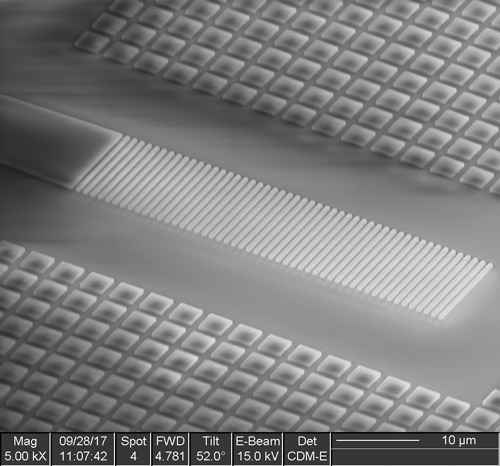
A scanning electron microscope image of the hybrid SiN-silicon grating fibre coupler from Leti that helps demonstrate the potential to produce a CWDM transeiver based on SiN
Leti scientists have also studied optimising bit rates for optical data interconnects based on silicon photonics, which underlined the importance of thermal issues, Wilmart said. His colleagues looked at a link carrying data from the electrical to the optical domain, encoding data with a ‘thermally-tuned’ ring resonator modulator. Such modulators incorporate heaters that control their resonance wavelengths. In particular, the researchers wanted to find out whether a 65nm lithography scale CMOS or 28nm SOI platform promised the best energy-per-bit ratio.
While the SOI platform was more energy efficient overall, the change in efficiency with bit-rate was more interesting. Between 12-22Gb/s the SOI device’s energy efficiency per bit remained largely constant when thermal tuning consumed 3mW. However, reducing thermal tuning’s power consumption consistently lowered the minimum energy consumption per bit, which was attained at low bit rates. The team therefore concluded that ‘further research should aim for lower tuning powers, instead of higher speed’.
Actively uncool
Tymon Barwicz, who leads silicon nanophotonic packaging research at IBM in Yorktown Heights, New York, observed that thermal tuning is a popular approach. ‘The heat itself is not as much of an issue as the electrical power consumption to supply the heaters,’ he echoed. ‘There are various design strategies there to try to achieve maximum tuning or trimming range, while minimising power consumption. It’s an interesting topic of R&D.’
In addition to lowering PIC costs by exploiting silicon, it’s easier to test devices on silicon wafers, and tests can be less intensive, thanks to the reliability silicon techniques bring. With photonic devices therefore becoming cheaper, the cost of packaging that manages heat flow becomes more significant.
However, silicon photonics reduces the pressure there, because it generates less heat than silicon microelectronics chips would, stressed Barwicz. He added that, currently, such photonic devices are typically positioned at circuit board edges, meaning that ‘the thermal aspects are not a significant issue’ for them.
Barwicz echoed Wilmart’s observation that significant problems arise with active photonic chips. ‘The light source is temperature sensitive – the efficiency of typical III-V active regions drops significantly when the temperature exceeds 70˚C,’ Barwicz said. Thermal management may be more critical in vertical cavity surface emitting laser (VCSEL) miniaturisation for high-speed modulation, where heat extraction is a key limitation, than in silicon photonics, he added.
Ryan Enright, senior member of technical staff at the Thermal Management Research Group at Nokia Bell Labs in Dublin, Ireland, also emphasised the different capabilities of PIC elements. ‘From a thermal perspective, we look at the increasing integration of optical and electronic components as the biggest challenge,’ he said. ‘These components have distinctly different operational temperature requirements dictated by performance and reliability considerations. Typically, active optical devices, like lasers and semiconductor optical amplifiers (SOAs) need to be maintained below 60°C, but silicon-based electronics are quite happy operating at 80-90°C.’
Ideally, cooling PICs shouldn’t consume any energy, Enright observed, but that’s not practical within some data centre optical communications applications that Nokia serves. ‘Due to standards-defined ambient temperatures and an adverse thermal environment within racks, we need to provision for the refrigeration of active optical components,’ he said. ‘Improvements in active optical device materials design to increase operational temperature is one way to improve the situation.’ Nokia can also look at removing parasitic thermal resistances between devices and thermoelectric temperature controlled refrigerators, and between refrigerators and the ambient environment.
Enright’s team is participating in the European Thermally Integrated Smart Photonics Systems (TIPS) project, which targets heat management issues in data centres. ‘In TIPS, we have been exploring the incorporation of single phase liquid cooling and device-level thermoelectric temperature control into silicon photonics PICs,’ Enright explained. ‘Specifically, we have been assessing the trade-offs between thermal performance and manufacturability, given the constraints of the overall silicon photonics fabrication process.’ The project concluded in January and Nokia has started building on its lessons other internal research efforts, Enright said.
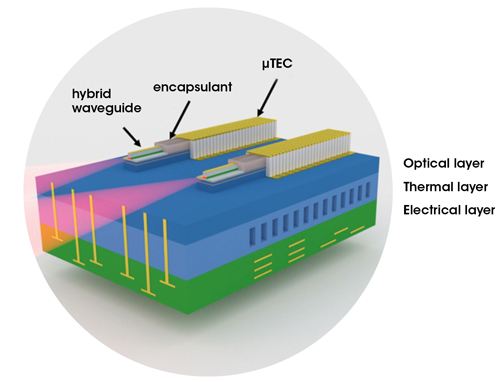
Thermally Integrated Photonics System (TIPS) conceptual architecture. A stacked optoelectronic architecture composed of: an optical layer with waveguides, passive photonic components, active photonic components and device-integrated thermoelectric cooling; a thermal layer acting as an interposer that contains embedded microfluidics; and an electronic layer containing analogue and/or digital electronic functionality
Thermoelectric cooling also offers interesting prospects in thermal tuning, which usually uses resistive heating. ‘We have been exploring the concept of device-integrated thermoelectric temperature control in our research,’ Enright revealed. ‘However, we are still in the research phase with regards to this technology so, for the time being, resistive heaters are the only practical thermal tuning approach, whether that be for lasers or optical resonators.’
Less stress
Issues due to diminished performance of active components now loom larger than the mismatch in coefficients of thermal expansion (CTEs) between InP lasers and silicon wafers they’re bonded to. The stress caused by one component expanding at a different rate than its surroundings ‘can be challenging’, Enright remarked, but he’s not greatly troubled by it. ‘Advancements in this integration strategy over the last decade can now routinely produce well-functioning active devices with a thermal budget of around 300°C during processing,’ he said.
Europe’s Waferscale Integration of Photonics and Electronics (WIPE) consortium is working on connecting PICs and micro-electronic integrated circuits (ICs) in this way. Led by Eindhoven University of Technology (TU/e) in the Netherlands and with six other partners, WIPE seeks to eliminate expensive and bulky wire bond connections to PICs.
WIPE bonds a thin InP membrane containing a complete PIC onto a BiCmos IC using an adhesive polymer, electronically connecting the layers with wafer-scale processing. This approach allows very short, high-bandwidth, interconnections. However, cooling both layers simultaneously is difficult, which brings thermal challenges that Manuel van Rijn, a TU/e PhD student, is studying.
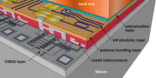
A cross-section for an integrated photonics/elecronic chip, showing the silicon CMOS layer and the InP photonic layer, with the metal interconnect stack and the polymer bonding layer in between, and heat sink on top
Van Rijn looks at average temperatures in both layers, for example, to cool and stabilise the optical layer at a temperature that keeps lasers and other components operating stably. But he has also simulated hot spots, such as those in the InP layer that would adversely affect the nearby electronics. Managing such hotspots requires a 2µm-thick gold heat spreader on the InP membrane, his simulations show.
However, the adhesive layer between the electronics and the photonics increase the thermal resistance between the heat sources and ambient air, van Rijn noted. And although InP chips themselves can also help spread heat, the thinness of WIPE’s membrane limits its ability to do this. ‘It is very important that we minimise the thermal resistance,’ van Rijn explained. ‘It’s also good to think about how we can help that horizontal spreading.’
The WIPE project is looking to create a design library of photonic/electronic standard modules using process design kits (PDKs) from European PIC and IC foundries. It will prototype a 400Gb/s transceiver for data centre applications. This includes an eight-channel transmitter that dissipates 2-3W of heat in the electronics and 2-3W in the photonic layer. Van Rijn’s simulations show this to be ‘challenging but doable’. ‘I’m focusing on thermal crosstalk between layers and reducing the temperature inside the laser cavity,’ he said. Meanwhile, IBM Research Zurich, in Switzerland, is designing the package and heat sinks.
Proceed with care
The density of heat sources on PICs is generally also increasing, van Rijn noted, creating higher overall temperatures that lower efficiency and create greater thermal cross-talk. That includes lasers for wavelength division multiplexing, SOAs for lidar sensing, and thermal tuners for silicon devices. This mainly affects the structures with dense SOA arrays and, currently, the density is limited by thermal issues. ‘We could improve this situation by improving efficiency of the SOAs, using heat spreaders to lower the thermal resistance to ambient and by using aluminium-based SOAs since they can operate at higher temperatures,’ said van Rijn.
WIPE’s use of thin InP membranes reflects how the industry deals with differences in CTEs when integrating active components with silicon photonics. ‘For the III-V chip, it all has to do with how you affix it and connect it to the photonic chip,’ Barwicz said. ‘The smaller the III-V chip, the easier the CTE mismatch is to accommodate.’
To help manage CTE issues in a different context, IBM has developed a polymer-based ‘compliant optical interface’ between standard optical fibres and silicon nanophotonic waveguides. ‘The compliant polymer interface helps with what is called chip-package interaction,’ Barwicz said. ‘The various CTEs of the various materials used in a package can create significant stresses within the package with environmental temperature cycling. This can lead to package failure with time. The soft connection of the polymer interface reduces those stresses and is expected to improve long-term reliability.’ IBM is commercialising this and its other silicon nanophotonic packaging solutions as a service at its Bromont, Canada, manufacturing site.
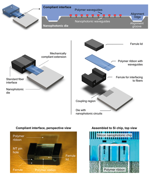
IBM has developed a compliant polymer interface to use in its silicon nanophotonics packaging to manage stresses within the package with environmental temperature cycling
One issue with using polymers to manage thermal issues is that they can break down at high operating temperatures. However, IBM’s compliant optical interface is designed to take even higher manufacturing temperatures into account. ‘The polymer we use is very resistant to thermal degradation,’ Barwicz said.
‘It can withstand typical solder reflow at around 250˚C without measurable damage. Note typical upper temperature of service can be in the 80-85˚C range, so it is not that high.’
While Barwicz is confident about the capabilities of such technology to handle existing thermal issues, the future brings greater challenges. ‘Once we bring the photonics, and especially the laser, closer to the microelectronic logic chip generating the data, the heat from that microelectronics chip could heat the III-V in the photonic device and reduce the light output notably,’ he said. ‘This is especially true down the road, where people contemplate embedding such high-power microelectronic chips with photonics in one module. Careful thermal design will be required.’