Portable, wearable and disposable could all be used when describing modern technology. It’s no surprise then to hear the same terms come up when exploring the innovations being made in spectroscopy, a field that has recently seen a new range of compact, affordable spectrometers based on emerging chip-level technology that allows them to be mass-produced in standard MEMS foundries.
With both industrial and academic groups taking their own approach to scaling the technology, use cases are being realised across various industries, spurred on by the reduced price tag and increasing availability of spectroscopic technology.
Testing for traces
Researchers at IBM’s Thomas J Watson research centre demonstrated a chip-based spectroscopic gas sensor recently, which is capable of detecting trace gases such as methane, in concentrations as low as 100ppm. The device is the direct result of a programme funded by ARPA-E, a research branch of US Department of Energy.
‘With methane being an incredibly potent greenhouse gas, its leakage poses hazards to the environment… Oil and gas industry operators therefore have an interest in ensuring they can detect, localise and repair the gas leaks occurring within their production, processing, and distribution operations,’ commented Dr Chi Xiong, a physical sciences research staff member at the Thomas J Watson centre. ‘Our mission is to deliver an entire methane detecting solution, including both the physical sensor and the data analytics that pinpoint the leak and quantify the leak rate.’
The IBM researchers have developed a silicon photonics-based spectroscopic gas sensor that combines a laser, a sensing waveguide and a detector all integrated on a 0.5 x 0.9cm chip, which can be manufactured using the same low-cost, high-volume manufacturing methods of silicon semiconductors. As a result, the new system could cost just a few hundred dollars, including a power source and housing.
‘With as many as one million oil and gas wells across the US, the volumes that these systems could be deployed in are huge,’ said Xiong. ‘There would generally be multiple sensors within each system, thus the volume of sensors deployed is also very large. This is where we think the silicon photonics sensor really has an edge, because it can be manufactured at large scales and therefore at low cost, while maintaining performance.’
In the next five years, networks of sensors like this miniature silicon chip trace-gas spectrometer, made by IBM Research, will help us "see" and reliably detect methane on-the-chip. (Image: IBM)
In contrast, the benchtop spectroscopic gas analysers available on the market – featuring large standalone lasers, prisms, mirrors and detectors – can cost tens to hundreds of thousands of dollars, making them unsuitable for high-volume manufacturing. These larger systems can offer parts-per-billion sensitivities.
IBM’s new spectroscopic gas sensor uses absorption spectroscopy, which measures how particular wavelengths of laser light are absorbed by molecules. Traditional set ups involve the laser light travelling through air, or free space, until it reaches a detector, which then measures how the light was absorbed by any gas molecules that might have been present, allowing their concentration to be calculated.
The new system uses a similar approach; however, instead of a free-space setup, the laser light – at near-infrared (NIR) wavelengths for methane detection – travels through a narrow silicon waveguide spiralling on the chip, which is 20 to 30cm in total length. While some of the light is trapped inside the waveguide, around 25 per cent of it extends outside the silicon and into the ambient air, where it can interact with any trace gas molecules passing nearby the sensor waveguide.
To compare the new device’s performance with that of a standard free-space spectroscopic gas analyser, the researchers placed the devices into an environmental chamber and released controlled concentrations of methane, finding that the chip-based spectroscopic gas sensor provides accuracy on a par with the free-space sensor, despite having 75 per cent less light interacting with the air compared to the free-space design.
While the new device offers higher levels of integration than free-space optical sensors, this does result in a reduced interaction path between the trace gas and the light, meaning the parts-per-billion sensitivities of benchtop spectroscopic gas analysers are currently unachievable at this scale.
‘You are limited to the interaction you can get on a centimetre-scale chip,’ Xiong explained. ‘On the silicon photonic chip, the light in the waveguides is also mostly confined within a silicon waveguide, which… can’t really be made any longer without compromising the signal-to-noise level at the detector, as light experiences propagation losses as it travels along the waveguide. This is a design trade-off we have to make when building integrated sensors – how much interaction you can achieve without experiencing too much loss.’
More applications for the new spectroscopic gas sensor could be enabled if its sensitivity was increased even further, according to Xiong, which the researchers plan to achieve using longer wavelengths in the mid-infrared range. ‘By using a wavelength of 3µm it would be possible to have a 100-times increase in sensitivity to methane,’ he explained. ‘This is a direction that we are excited about as it will require new sets of materials and a new set of challenges to overcome.’
While the new device can be manufactured predominately with standard high-volume fabrication methods, the IBM researchers have also developed their own unique process that allows them to integrate multiple photonics components onto a single chip.
‘We have invented a new packaging and assembly process that enables us to bring the laser onto the chip, which is one of the big challenges with silicon photonics and sensing, as silicon does not lase,’ Xiong explained. ‘We designed an indium phosphide (InP) gain chip and used a supplier’s standard manufacturing process to procure those as chiplets. We then invented a very special bonding technique to flip chip assemble these chiplets onto a silicon photonics chip containing the rest of the methane sensor components,’ Xiong continued. ‘Not only are they mechanically bonded, electrically and thermally but they also make sure the light can be coupled very efficiently with low loss from the InP chiplets onto the silicon photonics chip.
‘We’ve designed it so that this technology can be manufactured in a process that self-aligns the two chips together with sub-micron precision, so that a low-loss interface can be achieved without the use of high-precision pick and place tools. This assembly process can also be scaled up for wafer-scale processing,’ Xiong added.
IBM’s new silicon photonic methane sensor will be deployed in a number of upcoming oil and gas industry leak detection and quantification field tests this summer, the results of which will be very encouraging for the photonics industry as a whole, according to Xiong, as they will provide a practical validation of the capabilities of chip-scale optical trace gas sensor technology.
Making the small even smaller
Si-Ware Systems’ (SWS) spectroscopic scaling efforts have resulted in a miniaturised NIR spectral sensor featuring an entire micro interferometer integrated onto a single 1 x 1cm MEMS chip, with the company having reproduced certain benchtop spectrometer components in a unique confined format.
‘We’ve recreated the moving mirror – the motor is now a MEMS actuator, allowing the mirror to move forward and back – the silicon beam splitter and the fixed mirror [of a benchtop FTIR spectrometer],’ said Scott Smyser, executive VP of worldwide marketing and business development at SWS. ‘Getting all of these components on such a small chip is enabled through our SiMost process, which is at its core a standard MEMS process, with some additional IP concerning the design that allows us to instead integrate optics at this scale.
Si-Ware Systems' NeoSpectra Micro spectrometer can be mass-produced for consumer applications. (Image: Si-Ware Systems)
‘With a standard MEMS process – for example for an inertial sensor – you’re not using optics, so you’re not concerned about verticality or smoothness of the surfaces. For us, however, our mirrors have to be very vertical and smooth, and we have to be able to etch down at a pretty significant depth to achieve this… this is where some of our IP comes in, allowing us to do it with optics.’
These differences do not necessarily mean that SWS chips cannot be manufactured in a standard MEMS fab, using conventional components and processes, according to Smyser.
SWS’s first-generation product using the micro interferometer MEMS chip is the NeoSpectra Module, an FT-NIR spectrometer about the size of a deck of playing cards that also includes an electronics board containing a specially designed ASIC, a single InGaAs photodetector and optical fibres. The device started shipping in 2016 for approximately $1,000 and the firm has sold thousands of units. It has been integrated into systems such as handheld soil analysis tools and portable analysers for the oil and gas industry.
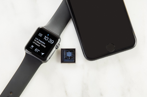
Through recent efforts, SWS has been able to scale this technology down even further to produce the NeoSpectra Micro, a chip-sized, OEM NIR spectral sensor with a core module size of 18 x 18 x 4mm, priced at around $100. The device was recently highlighted for winning SEMI’s Technology Showcase Award in Grenoble, France at the SEMI European MEMS and Sensor Summit 2017.
‘The NeoSpectra Micro was developed to bring spectroscopy even more so into the hands of consumers at a much lower price tag,’ said Smyser. ‘We’ve been able to do this through further optimisation of the optics and electronics, for example as opposed to using fibre to connect the MEMS chip to photodetector and the connector – as was done in the NeoSpectra module – we’ve instead gotten rid of the fibre and are now using plastic optics with mirrors.’
There are three pieces to the NeoSpectra Micro: The optical core module, consisting of the monolithic single-chip interferometer and a single element uncooled InGaAs photodetector; a proprietary ASIC; and an optical head – a mini optical structure for sample illumination and the collection of diffuse reflected light.
‘When a customer used the NeoSpectra Module to produce portable devices, they had to design their own light source and sampling interface, this has now all been integrated into the NeoSpectra Micro,’ Smyser said.
The NeoSpectra Micro has a spectral range between 1,350nm and 2,500nm and a resolution of 16nm, which is not as high resolution as a benchtop device, but is still enough to enable inline applications on portable consumer devices, according to Smyser, who explained that the device has already been designed into an iPhone case and used to perform tasks such as identifying the gluten levels in flour, or caffeine levels in coffee. ‘In the future consumers could use it to detect potential allergens in their food,’ he said.
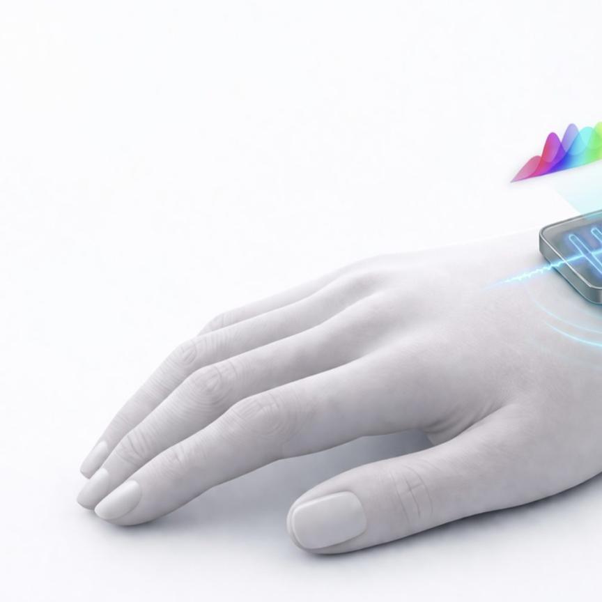
SWS also sees potential for the technology in wearable medical devices, as non-invasive biochemistry measurements can be performed using NIR spectroscopy, for example measuring blood glucose and alcohol levels.
‘As we continue to bring down the size and cost of spectroscopy with our spectral sensors, we’re enabling new applications and new use cases across multiple industries,’ Smyser confirmed. ‘What we will find is a lot of new applications developing as this technology gets out.’
SWS intends to shrink its spectral technology even further, with plans for a NeoSpectra Nano already on the company’s roadmap – a cheaper, smaller system that will be even easier to integrate into portable devices.
The increasing adoption of affordable chip-level spectrometers could prove beneficial to the photonics industry as a whole, according to Smyser, as their use of components such as photodetectors, plastic optics and mirrors will provide a boost to the photonics firms supplying them, thanks to the high volume of orders expected for the new technology.
A crystal clear approach
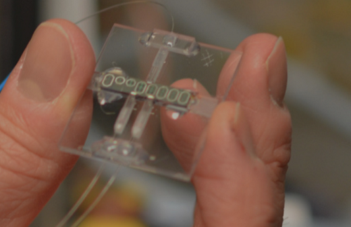
New York-based Chromation is taking its own approach to compact spectral sensing with the Chromation Spec, which, according to the firm, is the world’s first commercial photonic crystal spectrometer to be commercialised.
‘In the Chromation Spec, light travels through a fused silica die where it is structured by mirrors and absorbers along a folded optical path to a photonic crystal, which creates spectral selectivity,’ explained Chromation CEO Nadia Pervez. ‘This die is assembled with a detector with a simple stacked alignment to make a spectrometer.’
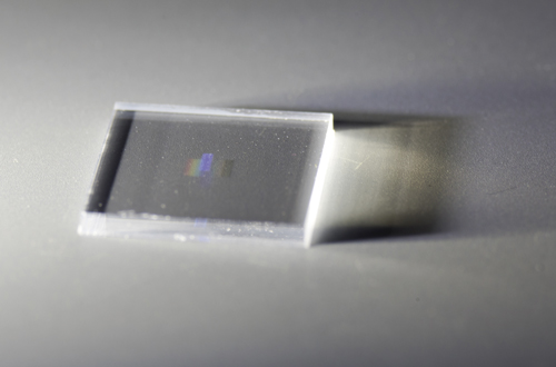
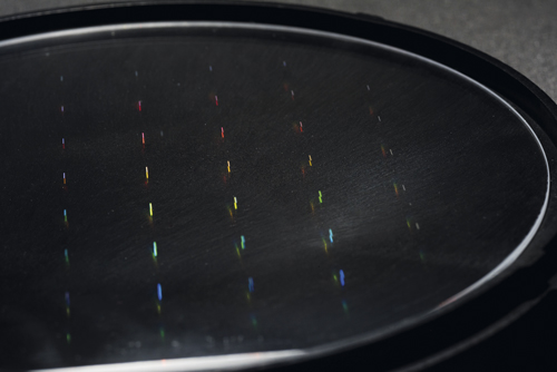
Fused silica die with photonic crystal. Light scatterred by the photonics crystal is visible as a rainbow. (Image: Ruby Tull Photography)
According to Pervez, Chromation’s design is based around scattering spectroscopy rather than absorption spectroscopy, using a single element to divide the incident light into all constituent wavelength bands at once. Scattering the incident light removes the need to re-image the input, while creating a spectrally selected output, as is the case with Czerny-Turner spectrometers, according to Pervez, which have to instead collect, collimate and reimage incoming light. In addition, by using non-imaging photonic crystal, less precision glass is needed, according to CTO John Kymissis, reducing the overall size and cost.
The features of the Chromation Spec are defined using wafer scale optical lithography processes and dry etch, Pervez noted. Fused silica was chosen for the substrates as it is transparent from UV to NIR, and is compatible with silicon production lines, she explained.
While the current generation of the technology offers broadband UV/VIS/NIR response from approximately 300-1,000nm, Chromation has already demonstrated its approach out to 10µm.
‘Similar designs can be used for longer wavelengths, outside of the fused silica transmission range, but they require other materials and processes,’ Pervez explained. ‘The choice of detector also becomes an issue – at a minimum you need to consider the value proposition of an inexpensive optical die matched to an expensive detector.’
While the Chromation Spec is currently offered as an evaluation board measuring 21 x 9 x 4.5mm, Chromation’s roadmap includes a chip version of the technology to address the growing demand from mobile, wearable and disposable applications along with extensions to longer wavelengths.
Scaling down this technology is not without its drawbacks, according to Pervez. ‘One of the trade-offs that we need to make in scaling down size is reduction in field of view,’ she explained. ‘The design rejects light outside of the target field of view, so it still is “point and shoot”.
Fused silica wafer with photonic crystals. The photonic crystals are the same but appear different because of the variations in viewing angle. (Image: Ruby Tull Photography)
‘It really depends on the application as to whether the small field of view is a feature or a drawback. It means we don’t collect as much light, but the light we do collect is spatially resolved.’
‘There are [also] trade-offs in throughput, resolution, and size for all spectral sensing technologies,’ added Kymissis. ‘What we offer is the best approach at the miniature size scale; it’s as spectrometers scale up that other approaches start to surpass us in performance.’
Superior scaling
Smyser, of SWS, explained that many spectroscopy players have been miniaturising their technology using discrete optics – reducing the size and amount of optics used – which can be quite limiting as discrete optics can’t really be scaled in terms of volume or cost.
In a 2016 paper published by the Institute of Electrical and Electronics Engineers (IEEE), Derek Kita, a fourth year PhD Candidate working at the Juejun Hu photonic materials research group at MIT, demonstrated that simply replacing the bulky discrete optical elements of conventional IR spectrometers with their on-chip counterparts, is not a viable route towards on-chip infrared spectroscopic sensing, as it cripples the system performance due to the limited optical path length accessible on the chip.
‘The primary issue with simply replacing components from free-space dispersive spectrometers with their on-chip (planar waveguide) counterparts, is that the spectral resolution of both dispersive and modulated (such as Fourier-transform) devices scales linearly with the device size, assuming a fixed spectral bandwidth,’ Kita explained.
The MIT group has therefore designed its own method of performing on-chip spectroscopy that it calls digital Fourier-transform (dFT) spectroscopy. ‘This technique uses time-domain modulation of a photonic Mach-Zehnder interferometer to perform very high-resolution spectroscopy,’ said Kita. ‘Unlike other tunable Mach-Zehnder structures that use thermo-optic or free-carrier-dispersion effects to modulate the phase of light, our architecture consists of a cascaded set of switches that physically alter the waveguide length difference between top and bottom interferometer arms.
‘With this architecture, each binary switch state corresponds to a unique measurement of the interferogram, so a simple 10-switch dFT spectrometer can offer 1,024 spectral channels, a figure that is already competitive with commercial free-space spectrometers.’
As with IBM’s, SWS’ and Chromation’s chip-level spectroscopic technology, the MIT group’s dFT architecture can be readily fabricated with standard photonic building blocks available at most foundries.
Other benefits include increased temperature stability, picometre-level wavelength resolution, and a large signal-to-noise ratio improvement, according to Kita, whose group recently demonstrated successfully working dFT spectrometer prototypes working in the telecommunication wavelength range.
The next step for the team is moving towards fabricating and demonstrating dFT spectrometers at other wavelength regions that are relevant to chemical and biological detection, such as NIR for Raman spectroscopy, as well as mid-IR for absorption spectroscopy.