To some, optical product buyers’ expectation that prices continually fall may seem a strange and unnecessary pressure on vendors. However, it’s a daily fact of life for the industry.
Product testing is an obvious opportunity to cut costs, according to François Couny, product line manager at test, monitoring and analytics solutions provider Exfo. Couny estimates that 30 per cent of the total cost of photonic chip production is driven by testing. But testing improvements for photonic integrated circuits (PICs) in particular are increasing speed, scalability and reliability while reducing operating expenses, he says. ‘That’s really the end game as manufacturers face the challenges inherent in global network transformation,’ stressed Couny.
Scott Jordan, head of photonics at Germany precision motion and positioning technology firm PI, sees a similar opportunity in aligning the parts of a device. He cites ‘many studies’ spotlighting this as the costliest part of manufacturing silicon photonics, for example. This doesn’t contradict Couny, Jordan stressed, but is part of testing costs, and ‘every step of photonic device manufacturing. Alignments must be performed a dozen times or more, starting at wafer-test and proceeding through the assembly and packaging process.’ PI therefore offers parallel gradient search optimisation (PGSO) alignment technology – which, Jordan says, reduces alignment costs by a factor of 100.
Such technology can help deliver scalable, flexible manufacturing automation that can reduce product prices, which Jordan sees as the greatest challenge facing the photonics industry. He compares the sector to the mainstream silicon semiconductor industry in 1984. ‘The rich ecosystem of toolmakers the semi folks take for granted today didn’t exist then, and it took a while for it to happen,’ Jordan said. ‘Back then, chipmakers had to commission custom tools or build them themselves.’ This is the photonics industry’s status today, he stressed. Yet companies like EXFO and PI are now seeking to provide testing and alignment tools that can enable the improvements the industry needs.
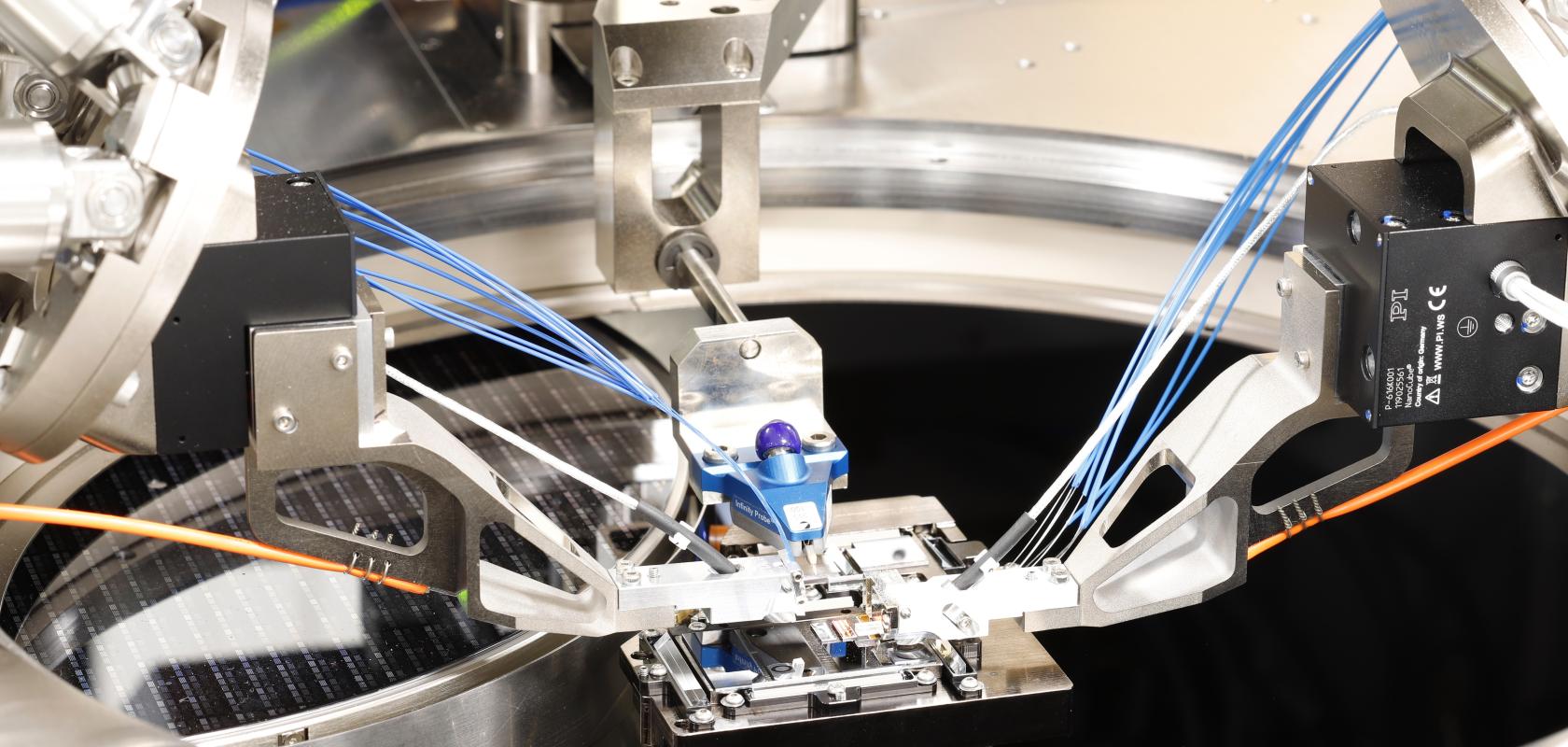
The Cornerstone silicon photonics rapid prototyping foundry at the University of Southampton, UK, exemplifies these needs. A key area that it focuses on is etching silicon wafer devices to realise photonic designs, explains Callum Littlejohns, Cornerstone’s coordinator. After every etching process, Cornerstone engineers must measure depth at several different points on a wafer. ‘Does it etch the entire wafer at the same rate?’ Littlejohns asked. If a wafer’s edges are etched faster or slower than its centre, engineers can change the etching recipe to rectify this. However, this may bring other problems, like changing the sidewall angle of silicon waveguides being made.
Tracking tolerances
Testing tools have helped Cornerstone build a library of recipe parameters to quickly fix such drifting processes, Littlejohns explained. Cornerstone uses critical dimension-scanning electron microscopy (CD-SEM) to monitor lateral dimensions during processing, like the width of a waveguide patterned by lithography. It also uses ellipsometry, exploiting changes in light polarisation to measure vertical dimensions during processing, like a waveguide’s etch depth. ‘In the case of CD-SEM, we are able to measure dimensions of features patterned into the photoresist coating on the top surface of the wafers before the next process step takes place,’ said Littlejohns. If needed, engineers can remove the photoresist and repeat it with modified parameters, which is ‘very valuable.’
The precision challenge varies according to the device type that Cornerstone is making. For example, to split optical power from one to two outputs, a 1x2 multi-mode-interferometer (MMI) is much more forgiving than a y-junction power splitter that does the same function. In the latter, there is often a tip narrower than 150nm between the two outputs, making variations of just 15nm significant.
The Cornerstone silicon photonics rapid prototyping foundry at the University of Southampton, UK, must address alignment precision challenges. (Credit: University of Southampton)
Littlejohns highlights that some photonics devices incorporate heaters that use temperature to tune the silicon devices’ optical properties and overcome such precision challenges. He describes a system containing 10 ring resonator devices, which should each have 200nm coupling gaps. After fabrication these gaps will in fact range between 190 and 210nm, so each device performs slightly differently. Separate heaters control each ring resonator to correct for this, which must be continuously powered up. ‘The cost of performing this type of correction is power to drive the heaters and design complexity in terms of the number of electrical contact pads needed to drive the heaters,’ Littlejohns said. Consequently, colleagues of the Cornerstone team within Southampton’s Silicon Photonics Group are working on a better solution, known as trimming.
Trimming permanently corrects fabrication errors, for example by implanting germanium ions to damage a silicon crystal, and selectively healing parts of it by annealing with a laser. To enable this, the team must continually measure to see when the device reaches the desired performance, and then stop annealing. Two fibres couple light into and out of the device to measure its resonant wavelength and quality-factor, while engineers use a third fibre for annealing. For this they use a wafer-scale-tester probe station like those supplied by Achim, Germany’s ficontec. ‘Using a trimming technique, there is a one-off overhead of initially tuning the device, but then during operation continuous electrical power consumption is not needed,’ Littlejohns said.
PI’s approach to resolving alignment issues extends digital gradient search technology that Jordan first developed and commercialised in the early 1990s. Originally, it addressed smooth, single-mode couplings, typically between devices and single fibres. ‘By comparison, today’s silicon photonics devices are largely multi-channel devices with highly asymmetric coupling profiles,’ Jordan explained. Using the old technique on these devices takes too long. Many different interdependent parts of the system must be tested one after the other. However, any changes made affect the other parts, so testing sequences must be repeated many times in loops. ‘That’s why we’ve seen industry chasing passive alignment techniques, where components snap together,’ said Jordan. ‘But they must be fabricated to sub-submicron tolerances. That isn’t easy or cheap either!’
Alignment stars
PI’s PDGS approach achieves a 100-fold speedup by eliminating the alignment loops. Jordan cites an example of a robot aligning an array device using old-style gradient search, where a first optical channel is optimised transversely. Later, to align other channels, the robot rotates the devices around the first channel’s optical axis. This damages the first channel’s transverse alignment, meaning the process must start again. PDGS enables both transverse and rotational alignment simultaneously, Jordan explained. Instead of a couple of minutes, this takes less than a second to do. ‘The PI systems automatically handle any geometric or optical dependencies,’ says Jordan. ‘It’s pretty magic stuff.’
Matt Adams, senior product manager at Viavi Solutions, notes that his company’s MAP photonics layer testing solution plays a role in tackling alignment challenges. It combines light sources, signal conditioning, switching/routing and power/spectral measurements. Together, these functions help tune, optimise, align and measure optical components, subsystem and modules. ‘Our MAP-based swept wavelength system, mSWS, is used extensively in waveguide production,’ Adams said. Basic power meter feedback can be used for coarse alignment, which plays an important role in optical loss and spectral response, he notes. ‘The mSWS can provide 100,000 data points in less than 0.5 seconds to characterise the magnitude and spectral shape of the loss profile,’ Adams explained. ‘This data can be fed back to third-party alignment equipment to finely optimise the fibre attach position.’
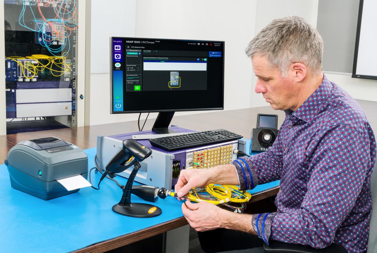
Fibre testing being conducted with the Viavi Passive Component/Connector Test Solution (PCT) on the MAP-Series platform. (Credit: Viavi Solutions)
Also spectral transfer measurements using the MAP mSWS can tune calibrate and align wavelength dispersive elements the modules, Adams said. Meanwhile, for applications like fibre attach, rapid, buffered measurements from the MAP optical power meter (mOPM) provide feedback to third-party alignment tools. And the company offers modules that can measure reflect power from a fibre-silicon chip connection to give a very sensitive measure of coupling efficiency. Manufacturers use such a platform as a process tool and a final test solution, Adams highlighted. However, it may be configured very differently between these situations. In configurations where alignment or tuning is being performed, the platform is typically controlled through PC-based automation and may include some hardware-based triggering, said Adams. ‘These tests are typically optimised to measure the same parameter as quickly as possible like power/insertion loss, reflected power or spectral shape/power,’ he explained. ‘For final test, there can be a much more diverse set of tools to measure a wider range or parameters.’
Meanwhile, optical interface visual inspection solutions such as those offered by Viavi can determine end-face quality of bare fibres, V-grooves and connectors prior to alignment and attach processes. The FV products are high-speed tools used to inspect optical interfaces, often incorporated into alignment stations. One reason for that is that it’s important to avoid contamination at optical interfaces, as it reduces test accuracy, commented Adams. ‘If the contamination becomes bonded between the fibre silicon interface, performance and reliability are compromised,’ he added.
Testing and alignment’s significance
Adams also highlighted the critical role that testing is playing as companies look to commercialise pluggable modules for use in data centres that comply with the 400ZR coherent optical interface standard. He notes that the Optical Internetworking Forum (OIF) standard for 400ZR has 21 subclauses that define the optical test requirements. These are intended to guarantee interoperability between vendors and generate error free traffic over the specified physical layers. Vendors need a range of products that can meet this specification on their own and are compact and easy to automate, Adams noted.
However, such standards also enable testing products from different companies to be integrated together, which Exfo’s Couny highlights as one of five key trends in PIC testing. The company therefore designs solutions to fit with this trend ‘enabling mix-and-match modular instrumentation from various vendors to be integrated to meet testing needs.’ That’s facilitated by another key trend, collaboration between testing solutions companies to improve their offerings. The trends also include implementing as much automation as possible, customising test environments, and designing products and processes to deliver improved testing. ‘To simplify the test process and maximise investment, we need to help customers keep testing top-of-mind from the design phase through to production,’ Couny said.
Among its portfolio of test and measurement equipment for PIC applications, Exfo supplies tools to characterise the optical spectrum of next-generation optical components, Couny continued. That capability is useful to component manufacturers, network equipment manufacturers, and labs at telecom carrier companies, from R&D through to deployment, he said. The company anticipates that in 2022 ensuring the viability of PICs through rigorous testing will become an even more important consideration for component manufacturers. That’s because they will be scaling their businesses to meet the demands of new technologies such as 5G mobility, high-speed broadband networking up to 800Gb/s, consolidated data centres, and edge networking.
Exfo has also released a series of instruments particularly suited for PIC characterisation. Such tools are designed to optimise testing throughout manufacturing, which allows companies to characterise PICs and transceivers fully and minimise failures during production or in the field. Such testing can help provide the extremely stable conditions needed for repeatable, high-yield processes. Couny cited the CTP10 modular passive optical component testing platform as an example. Working with swept tunable lasers, such a platform can measure insertion loss, return loss or polarisation-dependent loss over the full telecom wavelength range quickly and regardless of the device under test’s spectral characteristics. ‘This test equipment is already being used by PIC designers, manufacturers, and end-users to improve all testing requirements such as speed, accuracy, and repeatability,’ Couny stressed.
While testing is clearly critical, PI’s Jordan also reminded photonics companies to design for manufacturability to enable automated alignment. He noted that designs often fail to provide access to enable high-speed assembly tools to securely grip parts. ‘My advice to device manufacturers is to get manufacturing engineers involved early in device development,’ Jordan said.
‘You’d be surprised how often designs just get chucked over the wall into manufacturing.’
Diffuse reflectance targets aid the development and testing of lidar and ADAS systems
Target panels of diffuse reflectance provide known, stable reflectance levels regardless of the direction that the surface is illuminated from or the position from which it is viewed. This case study explains how this property is exploited in a diverse range of applications
In optics, we tend to think of reflectance in terms of specular or glossy surfaces, where the angle of incidence equals the angle of reflectance and your rays of light are well controlled. The reality is that very few surfaces, save for the most expensive laser optics, are truly specular. Most ‘glossy’ surfaces exhibit a small degree of near-specular reflectance, and we refer to this near-specular reflected (or transmitted) light as haze.
Imagine instead a material which is designed to reflect (or transmit) light equally in all directions, one that appears equally bright to an observer, regardless of the angle from which they view it.
This is the key attribute of a Lambertian reflector, named after the 18th Century Swiss polymath Johann Lambert, who described the concept of a perfect diffuse reflector in his 1760 book, Photometria.
A material that exhibits Lambertian reflectance is one which is a perfectly matte, or diffusely reflecting, and one which obeys Lambert’s Cosine Law. The cosine law tells us that for the case of reflected intensity (being the flux per unit solid angle), the magnitude of the light varies with the cosine of the angle that the surface is viewed from, compared to the surface normal. If instead we consider the reflected luminance (this being the flux per unit angle per unit area), the surface remains equally bright (same luminance) regardless of the direction of view or direction of illumination.
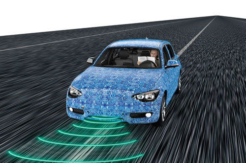
This property is exploited when testing the performance of machine vision or imaging systems. As with the human vision system, what counts with cameras is the luminance of light reflected from (or transmitted through or emitted from) a surface. The constant brightness of a diffusely reflecting surface ensures that the imager receives a stable level of light, regardless of the angle of view or illumination, which in turn greatly simplifies the calibration of camera systems. More recently, the use of diffusely reflecting materials has been exploited in the development and deployment of Lidar systems used in consumer electronic products and in the ADAS (Advanced Driver Assistance Systems) sensors used in autonomous vehicles.
Pro-Lite serves customers working in machine vision, image sensor, hyperspectral imaging, remote sensing, lidar and ADAS technologies with certified targets of diffuse reflectance made by our partners at Labsphere (USA) and SphereOptics (Germany). Labsphere’s Spectralon and Permaflect targets, as well as the Zenith and Zenith Lite targets made by SphereOptics provide near-perfect diffuse reflectance in the 250-2,500nm spectral range, and in particular at the critical NIR wavelengths used with lidar and ADAS systems.
Spectralon and Zenith diffuse reflectance targets are based upon proprietary sintered PTFE. In their natural (white) state, both materials provide diffuse reflectance over a 2∏ steradian field with a reflectance factor of up to 0.99. By doping the PTFE, grey-scale reflectance targets can be produced in levels from two per cent.
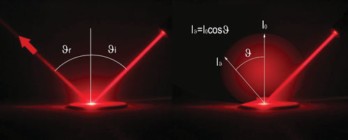
Figure 1: Specular Reflectance (L) Versus Diffuse Reflectance (R)
Labsphere’s Permaflect is a coating rather than a bulk reflector, but it also possesses near-perfect Lambertian reflectance in the UV-VIS-NIR and can also be offered both in white and various shades of grey.
For satellite ground-truthing experiments and for field trials of lidar and ADAS systems, the reflectance targets used need to be of a relatively large area. To that end, both Labsphere and SphereOptics targets are produced in standard sizes from a few cm up to 1m by 1.5m (1.2m by 2.4m for Permaflect) avoiding any seams (or gaps) between panels, which could lead to erroneous measurement data were you to assemble your own large area target panel from smaller tiles. Larger targets are needed in lidar and ADAS applications to reflect a representative number of points across the target surface over long-range test distances of several hundred meters.
Permaflect is a spray coating which allows it to be applied to large areas or 3D shapes, allowing it to simulate real world objects. Few real-world objects are flat like a target panel, so Permaflect coated objects allow for repeatable, near-Lambertian reflectance levels that can be applied, for example, to a mannequin to simulate a pedestrian.
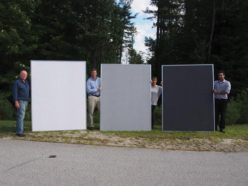
Figure 2: Labsphere Permaflect diffuse reflectance targets
All Labsphere and SphereOptics targets are available with certified calibrations, including reflectance at specified wavelengths, full spectral reflectance traceable to NIST and/or PTB, reflectance uniformity over the target surface and BRDF (bidirectional reflectance distribution function, a standard measure of how Lambertian the surface reflectance is).
Both Labsphere and SphereOptics maintain calibration laboratories that are accredited to ISO 17025 for reflectance measurements.