A global supplier of process control equipment for the semiconductor industry sought a compact, robust spectrometer to integrate into its overlay metrology systems. Here’s how Ocean Optics delivered a high-resolution, thermally stable spectrometer that provided accurate, reliable feedback on process deviations, helping to reduce errors and boost productivity
Research and development of semiconductor materials has led to remarkable strides in chip performance to keep pace with increasing demand for semiconductor devices. But as advances in chip size and performance become more challenging to achieve, semiconductor manufacturers have renewed their focus on improving fabrication efficiency and output quality. Streamlining processes, enhancing product quality and increasing wafer yields are evolving objectives.
Producing semiconductors is complex, with precise monitoring of fabrication processes integral to successful yields. As a proven analytical technology, spectroscopy is embraced by the semiconductor industry because of its versatility, simplicity and accessibility. Compact spectral systems are routinely used in semiconductor inspection, testing and manufacturing processes, where real-time, in situ analysis ensures reliable results. For example, even slight deviations in processes during fabrication can affect the electrical properties of finished wafers.
Optical emission spectroscopy (OES), reflectance and transmission are among the spectral techniques utilised by semiconductor process equipment providers to manage critical manufacturing steps including plasma monitoring (Figure 1) and endpoint detection. OES can identify materials in the plasmas that manage deposition and etching. Reflectance and transmission are often used for thin-film thickness measurements.
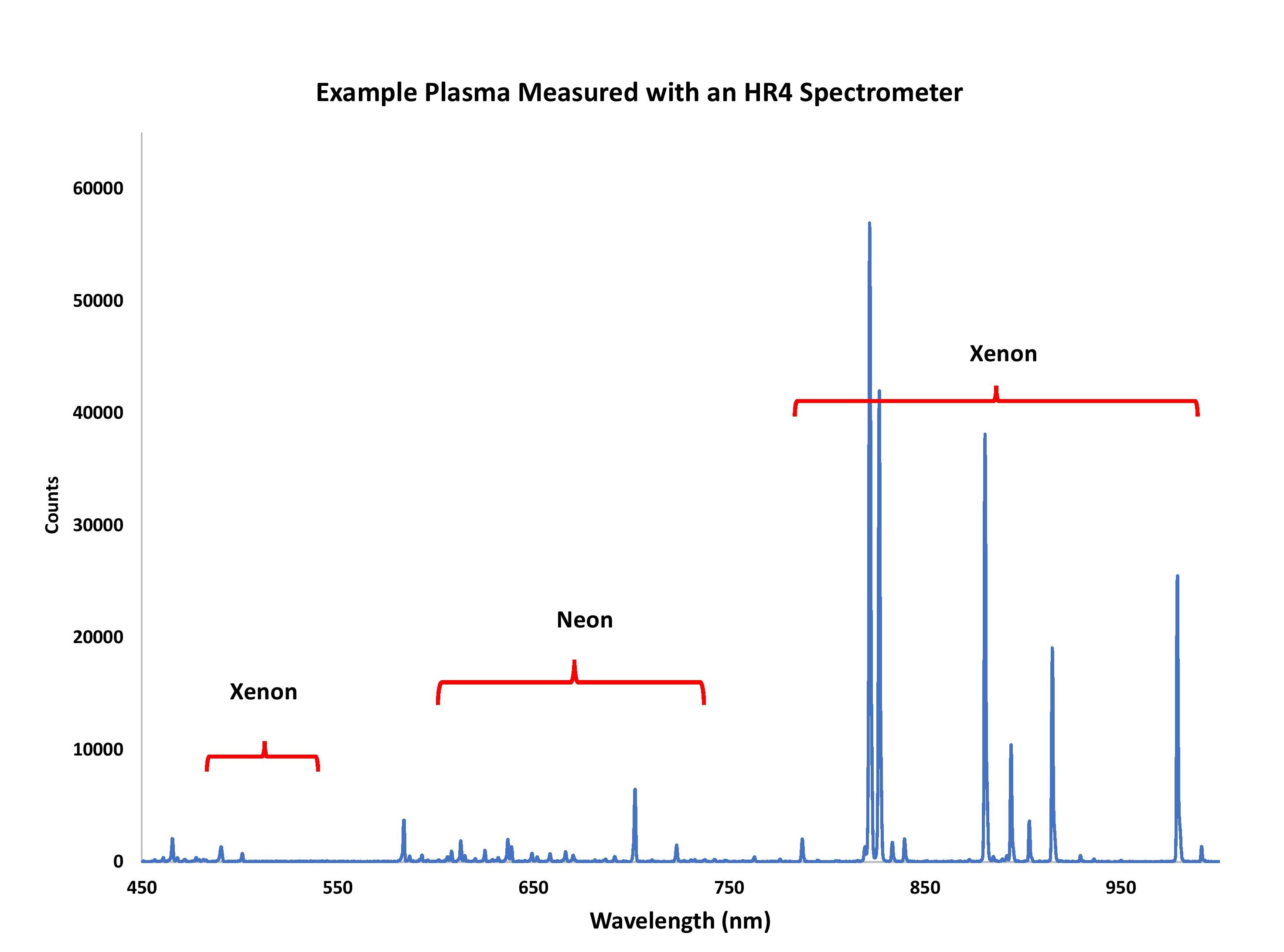
Figure 1: A high-resolution, thermally stable spectrometer is ideal for monitoring the emission peaks of gases used in semiconductor and other manufacturing processes
Addressing semiconductor processing challenges
Ocean Optics has a long history of supporting semiconductor process equipment suppliers that investigate materials and take on challenges related to plasma etching and deposition, overlay control, and plasma ashing and cleaning.
In the case of the overlay control system customer, the goal was to deliver a robust spectrometer easily integrated into the customer’s system and capable of providing reliable, high-resolution results over time and temperature changes. This is significant because spectral wavelength drift can produce measurement errors that carry through to the algorithmic modelling the customer uses to control key processes.
The customer needed a precise, process-ready spectrometer. Having an existing Ocean Optics spectrometer distinguished by its optical resolution performance was a great start. Add in a multidisciplinary team with expertise in opto-mechanical design and testing to re-engineer the spectrometer for an added layer of thermal wavelength stability, and the result was a solution that met the customer’s needs for peak wavelength accuracy and measurement repeatability.
An additional benefit of Ocean Optics’ successful spectrometer redesign was elimination of more intrusive and less easily managed approaches to maintaining thermal stability in the set-up. This sped up development and made the integration simpler to manage. Also, because Ocean Optics has a close partnership with the customer and had collaborated with them on other projects, the spectrometer design changes were accomplished within a short timeframe, and at reasonable cost.
Additional process monitoring applications
With better control of semiconductor processes, manufacturers can reduce interruptions caused by errors, produce less waste, and deliver higher-quality output. For example, when spectroscopy-based endpoint detection is used in metrology systems for overlay control, the endpoint can identify when an etched film has cleared the underlying film, which indicates the next step in the etch process to take.
Spectroscopy also makes endpoint detection more precise, enabling the design of more intricate wafer shapes and patterns. Because manufacturers can more accurately stop and start production processes, smaller features can be made with fewer errors and less unusable space on the wafer. Also, with a more accurate endpoint, thinner layers of materials can be used, even as those materials generate faint, difficult-to-discern spectral signatures and reveal closely aligned spectral peaks.
Ocean Optics has provided spectrometers for plasma monitoring applications, with OES, a technique commonly utilised for endpoint detection. For example, detection of a drop-off in certain plasma species can be an indicator in etching processes that action is needed to prevent damage to the wafer.
Leveraging the power of light
By customising high-performance spectrometers, Ocean Optics delivers the spectral acquisition speed, optical resolution and thermal stability so critical to monitoring semiconductor processes. With flexibility in the company’s hardware and depth to the team’s application knowledge, Ocean Optics provides solutions that process equipment suppliers can use to improve and refine the technologies they offer to the semiconductor industry.
Further information
Find out more information about Ocean Optics’ expertise in the semiconductor industry.