While epitaxial regrowth technologies for indium phosphide (InP) are relatively mature and can already be used to produce a range of building blocks for photonic integrated circuits (PICs), such circuits can only serve a limited range of wavelengths and applications.
Richard Hogg, CTO at III-V Epi and a new Professor at Aston University’s Institute of Photonic Technologies, told EO that the key to serving a much wider range of futuristic technologies and applications using cost-effective, highly capable PICs and semiconductor lasers, lies in the epitaxial regrowth of gallium arsenide (GaAs). However, current regrowth technologies are not yet mature enough to produce GaAs-based PICs at the volumes and cost required to address such markets effectively.
Hogg is therefore working with his colleagues at III-V Epi to further improve epitaxial regrowth processes for GaAs materials. While the company has indeed made progress in developing its own know-how in the regrowth of GaAs-based components over several years, Hogg says there are still significant challenges to be overcome before the required maturity level of GaAs epitaxial regrowth can be reached.
EO: Could you elaborate on why there is a need for mature GaAs epitaxial regrowth?
RH: While one of the first laser diodes was actually made out of GaAs materials, attention quickly switched to InP when it was recognised to be able to hit 1.2-1.7µm wavelengths, within which is the key 1.3-1.5µm needed to achieve single-mode fibre optic communications in silica glass with minimal loss and dispersion. Consequently, epitaxial regrowth processes for InP lasers saw rapid development to match that of the accelerating telecoms market at the time. It thus became a very mature technology, while GaAs remained much less so. InP lasers have since gone on to commonly serve applications involving telecoms, datacoms, 5G and co-located optics.
Current InP device manufacturing technologies involve multiple epitaxy (additive) and fabrication steps (lithography and subtractive etch) to form the semiconductor laser. These technologies contrast with the more basic ridge-laser structures, where one epitaxy step is followed by subtractive etching to form a waveguide, with passivation and isolation to produce electrical contacts (see Figure 1). For InP devices, these epitaxial regrowth processes enable a range of photonic integrated circuit (PIC) building blocks to be produced, such as low loss distributed feedback (DFB) and distributed Bragg reflector (DBR) sections; gain and passive sections; and buried heterostructures for low optical loss and enhanced heat extraction.
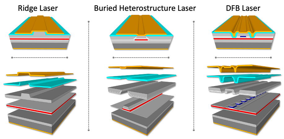
Figure 1: Example of a simple ridge laser, epitaxially regrown buried heterostructure laser, and epitaxially regrown DFB laser (Image: III-V Epi)
However, you could now make the argument that the kind of applications InP-based technologies are used for are becoming saturated, to the point where it’s now quite difficult to enter these markets without already having a solid background in InP technologies and manufacturing processes.
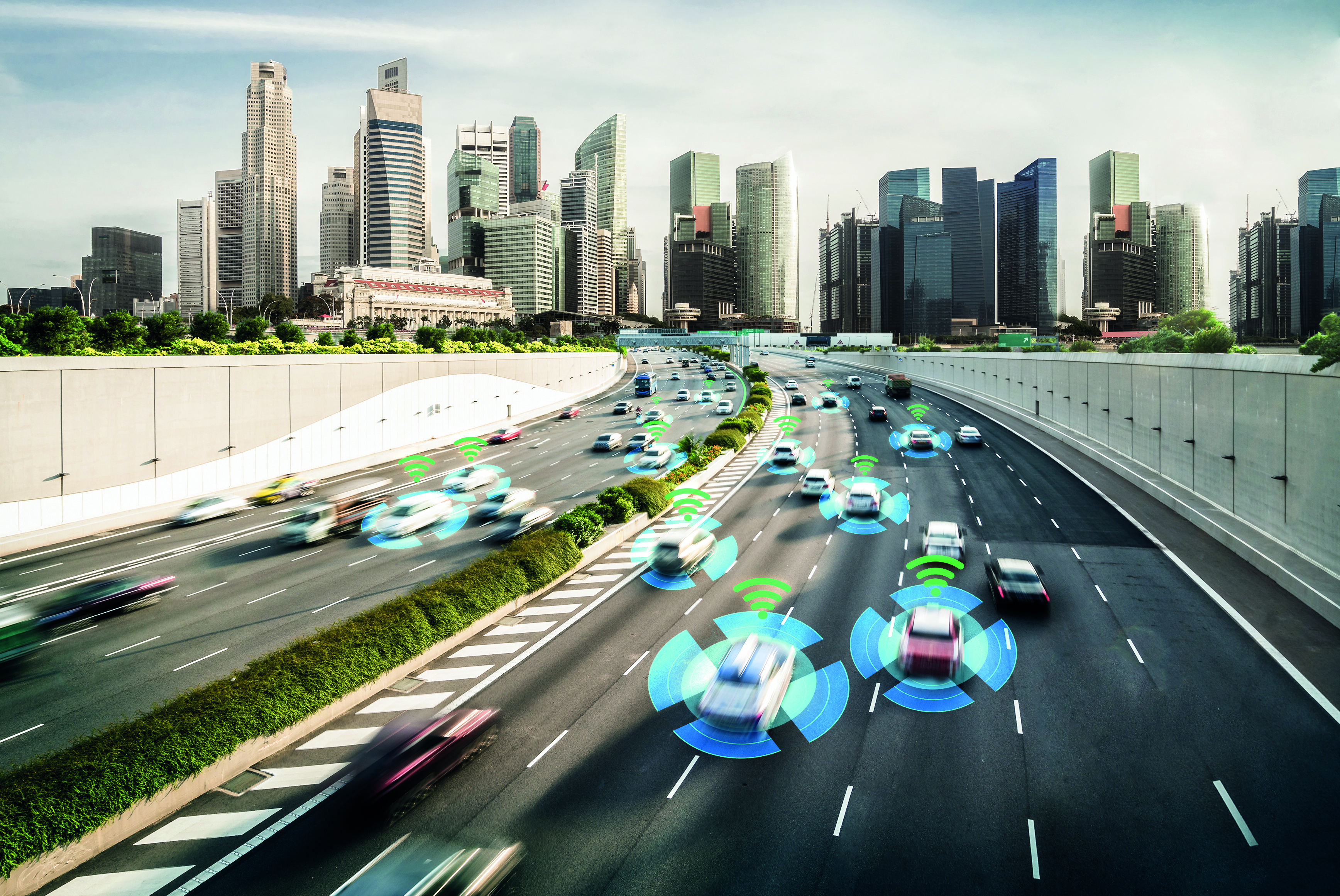
This has coincided with the emergence of new, advanced laser technologies over the past decade for applications including silicon photonics, industrial manufacturing and sensing, biomedical imaging, data storage and optical datacomms, displays, lidar, and the numerous quantum applications now being commercialised (e.g. atomic clocks and quantum computing). Many of these applications operate in the wavelengths served by GaAs material systems, which range from red (650nm) quantum wells, to near-infrared (1,300nm) quantum dots. GaAs-based technologies are therefore being increasingly recognised as the key to better serving such applications, as well as those in positioning, timing, health monitoring, autonomous vehicle sensing, and drone guidance.
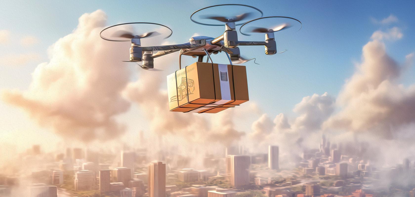
Mature GaAs epitaxial regrowth technologies could also deliver compact PICs for autonomous vehicle guidance (Image: Shutterstock/Blue Planet Studio)
However, for this growing number of applications opening up in the GaAs material system, the demands on the required photonics devices are ever increasing. People are looking for single frequency devices with high efficiency, high power, narrower line width, all while being mass-producible and costing only dollars to make. So all these kinds of requirements push the technology to require improved laser diode operating characteristics, and some form of integration – such as that already achievable with InP materials. This creates the need for mature GaAs epitaxial regrowth processes to produce the aforementioned PIC building blocks.
With GaAs still forming a much less mature material system, particularly in the regrowth technology areas, it has now come along as a newly-revived focus area for research and development.
EO: Why is epitaxial regrowth the best-suited process to unlocking GaAs-based photonics technologies?
RH: To achieve the best device performance, two things that are particularly essential are reduced optical loss and greater heat dissipation. Epitaxial regrowth achieves both of these while also addressing the ever-increasing demand for photonics integration.
As noted earlier, for InP it enables the production of PIC building blocks, such as DFB lasers (see Figure 2) and buried heterostructures.
![Figure 2: Distributed feedback (DFB) lasers manufactured by epitaxial regrowth [Credit: III-V Epi]](/sites/default/files/inline-images/Figure%202_2.png)
Figure 2: Distributed feedback (DFB) lasers manufactured by epitaxial regrowth (Image: III-V Epi)
For DFB lasers, initially the lower cladding and active elements (quantum wells) of the laser are epitaxially grown on a substrate. Epitaxial regrowth is usually performed by a metal-organic chemical vapour deposition (MOCVD) machine, which deposits semiconductor layers onto the substrate surface and grating. A cladding and cap layer ‘sandwich’ the active region with the DFB grating of the laser. This provides optical confinement and guides the light, which is emitted from the laser's facet. Within the process, a range of parameters can be controlled precisely, such as temperature, supply of reagents and pressure, to achieve the correct material properties, crystalline quality, and uniformity across the wafer. Dopants can also be introduced to ensure the required conductivity. A grating structure is then formed in the wafer substrate surface, using electron beam lithography and etching to deliver the DFB laser mechanism. This produces the correct period and depth of grating for the optical properties required. From here the wafer may be processed into an individual laser die, in the form of a ridge waveguide laser.
Alternatively, the wafer may proceed through other epitaxial regrowth steps to make a buried heterostructure (as shown in Figure 3). Here, optical confinement is much gentler than for a ridge laser, and current confinement is achieved through either a blocking p-n-p-n structure, or making the overgrown material semi-insulating, such as through doping with iron. Buried heterostructures allow improved heat extraction and hence greater output power. They also allow more symmetrical output beams, resulting in lower power loss in the subsequent optical systems and reducing the costs to fibre-package.
![Figure 3: Epitaxial regrowth steps for producing a buried heterostructure [Credit: III-V Epi]](/sites/default/files/inline-images/Figure%203_1.png)
Figure 3: Epitaxial regrowth steps for producing a buried heterostructure (Image: III-V Epi)
This is why epitaxial regrowth is important, especially with these applications opening up in the 650-1,300nm range and performance demands continuing to increase here. The photonics and semiconductor industries are therefore working to improve epitaxial regrowth and get GaAs-based technologies down to small enough packages where they can be used in a wide range of modern technologies and applications. GaAs-based PICs need to get to the point where they’re pea-sized and cost a dollar for them to end up in consumer technologies, and that's the reason all this research is taking place.
EO: What challenges are currently hindering the maturing of GaAs epitaxial regrowth technologies?
RH: Aluminium GaAs is commonly used as one of the materials being etched or regrown as it’s a high-bandgap, low-refractive-index material used for waveguide structures in lasers. Aluminium is also excellent as it's almost lattice-matched to GaAs, so you can use any aluminium composition you like to engineer your band structure and your refractive index profiles. However, while aluminium is so beneficial, it’s also problematic in that aluminium easily forms an oxide that is very difficult to remove. So there's a risk that you introduce defects within your device from an aluminium oxide blob disrupting the crystal lattice. It is therefore essential to minimise aluminium exposure.
There are a number of ways being used to work around this issue. For example, at III-V Epi we are able to perform in situ etching to remove any aluminium oxide created. However, this creates an additional challenge, as GaAs-based materials are also susceptible to damage from accidentally etching through the active regions of quantum wells.
Left: A GaAs-based laser made by III-V Epi using special “marker” layers to track the regrowth front Right: A novel, GaAs-based PIC device developed by III-V Epi (Images: III-V Epi)
An alternative might be to use gallium indium phosphide (GaInP), which offers a big band gap, but you've only got one choice in that there’s one gallium and one indium composition that give you a lattice-match to GaAs. This puts limitations on the parameters of your device design, and you might not like some of the choices this imposes on you.
So the wider semiconductor and photonics industry are working to overcome or work around these challenges that come with aluminium. While some are choosing to use GaInP and be stuck with the limitations it imposes on their device design, others are using aluminium GaAs to achieve a lot of flexibility in their device design, but then have to pay the price in avoiding the exposure of aluminium and subsequent creation of oxide.
EO: Once the required level of maturity has been reached, what would this mean for photonics and society as a whole?
RH: If the challenges surrounding GaAs epitaxial regrowth were solved, which I can see happening within the next decade or so, a myriad of futuristic, almost science-fiction-like devices would be unlocked based on new sensing/imaging technologies, which themselves are built on a foundation of mass-produced GaAs-based PICs with exceptional operating characteristics.
Such PICs would be deployed on an increasingly larger scale, culminating in their integration across smartphones and other consumer electronics. This could lead, for example, to more advanced health monitoring capabilities being developed for smartwatches and smartphones. For example, OCT technologies could be dramatically reduced in size and integrated into your phone or laptop.

Compact PICs enabled by mature GaAs epitaxial regrowth could also enable smart health monitoring applications in consumer electronics (Image: Shutterstock/Sun Image)
In addition, more advanced data transfer and storage, computing, timing, positioning, and autonomous guidance systems would become available. For example, tiny atomic clocks that enable devices to use 6G and 7G. This is because a lot of systems currently have their own clock recovery mechanisms, which is important for locking into the correct clock frequency and obtaining the right information from a data stream. With current technologies, the required clock recovery for 6G and 7G would likely be too expensive and power-hungry for consumer devices. GaAs-based PICs could deliver this capability in a far more efficient manner.
In addition, high-power CO2 and fibre laser sources, such as those used in materials processing, would gradually be replaced by more-efficient GaAs laser diodes. However, generating kilowatts of optical power will also result in a similar amount of thermal power being generated, and so excellent heat extraction will still be required.
Ultimately, this is all about enabling inventors to have the toolkits that don't limit their imagination. If you want a monochromatic light source offering spectral purity, high power, and the opportunity to make a photonic integrated circuit, then mature GaAs epitaxial regrowth technologies are inevitably required.
Professor Richard Hogg is CTO at III-V Epi and a new Professor at Aston University’s Institute of Photonic Technologies