It took decades to realise the current cutting-edge optical projection lithography technology – but semiconductor companies already want the next generation.
Customers of ASML, which sells these lithography systems, say that they would already adopt the new generation if it was available. That is according to Christophe Fouquet, executive vice president for ASML’s extreme ultraviolet (EUV) lithography programme.
‘There was a lot of customer praise of how they have used EUV to simplify, going from more than three masks to one and seeing defect density benefits,’ Fouquet said. The search to shrink components further is already undoing those gains. ‘Some today already require more than two masks for EUV. They would prefer to simplify,’ he added.
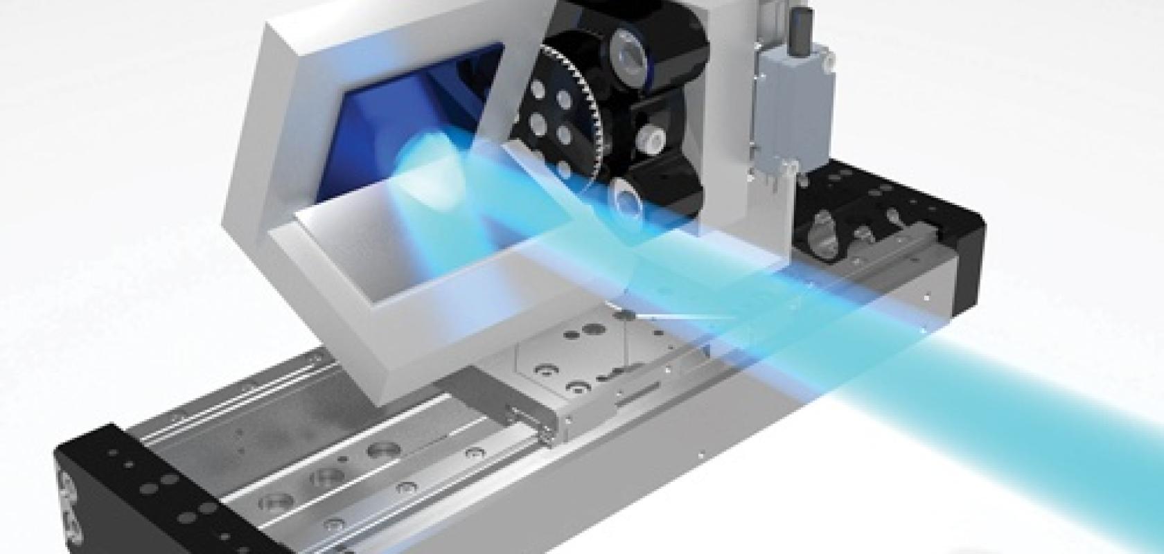
Masks define spectacularly tiny component and circuit patterns that ASML’s TwinScan NXE:3400C tools create by exposing photoresist material coated onto silicon wafers to EUV light. Exposure modifies the resist, before engineers wash away unwanted material, and plasma etch chip design shapes. EUV lithography has enabled Samsung and Taiwan Semiconductor Manufacturing Co (TSMC) to continue to shrink their transistors, entering volume production on the 5nm node. This is incredibly small, as just 10 silicon atoms might fit in a 5nm space.
The TwinScan NXE:3400C exploits the Rayleigh criterion, the formula that sets the minimum physical limit for resolvable detail. To reduce the resolution limit through the Rayleigh criterion, options include reducing wavelength and increasing numerical aperture (NA).
NA characterises the range of angles over which the system can capture and transmit the information contained in the diffracted light that occurs when light strikes the mask and is relayed to the projection optics.
EUV reduced the wavelength used from 193nm to 13.5nm. The next step will be to increase NA from 0.33 to 0.55. ASML and other firms are now battling to overcome the challenges needed to achieve this in the next two or three years.
Fouquet highlighted the biggest change needed to achieve high NA is a complete optical system redesign. ASML is doing that redesign in partnership with Zeiss in Oberkochen, Germany.
‘We are looking at much larger and asymmetrical mirrors,’ Fouquet said. ‘The methods to calibrate and manufacture those mirrors are completely different from anything we have done before. As we speak, we have many mirrors that will be used in high NA in production at Zeiss, because of the time it takes to get the technology in place.’
This optical arrangement will only be able to cover half the field of semiconductor devices that existing EUV techniques can, which would slow down the process. To compensate, ASML will develop high NA systems that move the reticle masks that define the lithography pattern with acceleration that is four times faster than existing EUV lithography systems.
Douglas Guerrero, senior technologist at US-headquartered lithography material supplier Brewer Science, said that unlike previous lithographic transitions, ‘what we’re encountering here is a lot of new inventions. A tool that can do high numerical aperture is a massive engineering undertaking to put together’.
Guerrero works at the imec semiconductor research lab in Leuven, Belgium, exploring the issues high NA technology faces. But he noted that only two places can do high NA EUV lithography, the Lawrence Berkeley National Lab, in the US, and the Paul Scherrer Institute in Switzerland.
Making every photon count
One materials challenge is that photoresist must be thinner to maintain the aspect ratios that high NA EUV lithography will enable. Patterns formed from thicker layers can collapse. But Guerrero stressed that thinner layers can pose challenges for commonly-used chemical amplified photoresist. They absorb fewer photons needed for photoresist deprotection.
One technology that has emerged to resolve this issue is metal oxide resist, from US-based Inpria. It readily absorbs photons, even in thinner layers, Guerrero highlighted. However, the shift to high NA will also help somewhat. ‘You will have a higher number of diffractive orders going into the imaging system, which means more photons,’ said Guerrero. ‘More photons mean fewer stochastic variations, less roughness.’
Lam Research is working to address this problem, explained Rich Wise, vice president and product line head for dry photoresist at the California-based firm. Photoresists need to be deposited in high resolution, enabling small features, with low line edge roughness (LER). They should also be highly sensitive, hardening on exposure to very few photons. But obtaining high resolution and sensitivity, and low LER, is difficult, Wise said.
Therefore Lam has worked with imec and ASML to develop a new type of resist, called dry resist as it doesn’t use solvents. It’s formed from reactive metalorganic precursors in the vapour phase, with thickness controlled by deposition and development time, that produces a high density of photosensitive clusters.
This new photoresist is therefore highly absorbing for EUV photons, Wise said. ‘Lam’s dry resist is a fundamentally different kind of resist, and the solution needed for high NA to be implemented,’ he explained.
‘Importantly, it allows resist height scaling to address the smaller depth-of-focus. Our dry resist eliminates the resist blur associated with chemically amplified resists, and we’ve already demonstrated resolution down to 18nm pitch, near the limits of the next-generation of lithography equipment. Dry process improves defect-free printing margin, which is important for smaller dimensional ground rules printed by high NA.
Multi-patterning in EUV
Another key feature of resist for higher numerical apertures, said Wise, will be satisfying higher resolution requirements to reliably capture enhancements in imaging. Companies are already adding complexity to EUV by incorporating the kind of multiple patterning approaches that can shrink the devices made through lithography further, he said. ‘We see multiple patterning continuing to play a role similar to the transition from immersion to EUV, where in many cases EUV implemented multiple patterning in analogous ways to previous generations,’ said Wise. ‘The industry has become adept at implementation of multiple patterning to enable hyper scaling beyond the Rayleigh criterion limit, and we see this continuing.’
Guerrero said that other problems occur because many properties of materials Brewer Science supplies change as the layers get thinner.
‘Brewer Science has always worked below the resist layer, before the imaging layer,’ he said. ‘In some cases, we can reduce the dose required for patterning, and we provide very strong adhesion to the resist. Our roadmap is to look in the next two years at how these materials’ properties change as you make materials thinner.’
Brewer Science’s adhesion layers can help prevent pattern collapse, in which photoresist at these small sizes becomes unstable. However, Guerrero noted that much attention is being paid to the causes.
‘When you have pattern collapse, part of the problem comes from the develop process,’ he said. ‘The capillary forces of water pull those small structures together and make them collapse.
‘So we can ask what develop processes will be needed? Maybe a non-aqueous system, something that has less surface tension. Inorganic metal oxide resists use non-aqueous solvents.’
John Petersen, principal scientist at imec puts the challenge of progress towards smaller patterns into striking context. Devices made using high NA EUV lithography, he explained, will be exposed to one-fourteenth of the number of photons of devices that were being made with 193nm argon fluoride-based excimer lasers.
‘We have to have a long enough exposure to reliably relay that information,’ he said. ‘Otherwise we’ll see stochastic print failures, which, especially as we get to the smaller features, are a relatively huge deal.’
These random pattern changes might create a bridge where there is a gap, or vice versa, or to missing or merged patterns like vias. Currently, it happens about once every billion pattern pixels but needs to be down to less than once every trillion for logic to yield. As such, Petersen and his colleagues are studying the physical processes happening when atoms absorb EUV light to cause these stochastic failures using spectroscopy. The imec team hypothesises that EUV causes electron ionisation within resist materials that lead to the stochastic failures, and is exploring how to prevent them.
EUV is here to stay
To tackle these problems, imec has set up AttoLab, which uses a 13.5nm high harmonic generation source from KMLabs to explore high NA conditions. This differs from the approach used in ASML’s lasers, which vaporise tin droplets to produce EUV light. In February AttoLab demonstrated printing of 20nm pitch line/space patterns using interference lithographic imaging of a metal-oxide resist.
‘These sources are not going to be used for commercial lithography, there’s just not a way we can ever get the throughput,’ Petersen explained. ‘We’re set up to image anywhere from 40nm pitch down to 8nm pitch. We have plans to use it to screen resist on 300mm wafers to help people develop the high NA materials, but we also want to use it to help develop etch processes and metrology. For the photoresist we can approach the actual event when the photon is first absorbed and the first electrons get released.’
Petersen said that imec should formally commission its AttoLab high NA tool emulator in the summer. That will allow it to prepare for 2023, when the first high NA laboratory, a joint venture between ASML and imec will come online.
‘We hope to get about a year and a half of work done, and in that time, we can help that ecosystem develop,’ Petersen said.
Yet he is unable to predict which materials might ultimately be successful. ‘Every solution is on the table,’ he emphasised. ‘We’re in uncharted territory right now. It took over 10 years to go from the first ASML EUV scanner to the production tools. And now we’re trying to do that in three years, with the high NA tool. That’s monumental. That’s the magnitude of the problem that we have. And that’s the reason for our laboratory.’
Fouquet says that as well as getting access to ASML’s 0.55 NA EXE5000 prototype tools through the demo lab, some of the first customers will be shipped them in 2023. The tools should be qualified in 2024-2025, with high volume manufacturing situation in 2025-2026. ‘This range also matches our own capability to ramp those tools,’ Fouquet said. ‘It is always two, three years at ASML to reach the number of tools you need to support complete volume production.’
He believes reducing the number of masks chipmakers use will be strong motivation for them to adopt the tools quickly.
‘They have learned to deal with more complex processes, but these usually come at the cost of defect density performance,’ he said. ‘When they qualify high NA, and they believe that the tool is ready, reliable and economically viable, then of course, they will want to remove this complexity.’
That will be possible rapidly because it was only the unusually unique challenge of developing the EUV source that slowed adoption. ‘It took us a long time at ASML to reach the right productivity level,’ said Fouquet. ‘It took us many, many years to go to 250W, which was the threshold to make EUV economically viable. Now, the source is there. What we have to do is get the optics, get the platform, the stages, put it together and reach the right level of availability. But that’s much more of an evolutionary step than introducing EUV was.’
He stressed that the close connection between the current generation of EUV lithography tools with 0.33 NA and the new high generation will help this processs.
‘High NA will benefit from all the work we have done in the last few years on EUV,’ he said. ‘As a result, we expect smoother insertion at our customers.’
Fouquet added the current and upcoming platforms will then be able to support semiconductor manufacturing for a long time. ‘We have ideas to extend the technology,’ he said. ‘It took us a while to come to this platform. Now we see it being a very important component of the industry for at least the next 10 to 15 years.’