Extreme ultraviolet (EUV) lithography, which will enable semiconductor fabs to pattern ever smaller feature sizes on silicon chips, is on the cusp of moving to high volume manufacturing, if reports from ASML and the industry at large are anything to go by. The lithography system provider, ASML, has sold two of its fourth generation EUV systems, the NXE:3350B, to Taiwan Semiconductor Manufacturing Company (TSMC), a contract manufacturer of silicon chips.
The NXE:3350B is the first of ASML’s systems specified for volume production of silicon chips. Its third generation system has been ordered by 11 semicon companies to date, which are using it to get an understanding of the lithography tool in order to fine tune their production processes and start getting their factories ready for EUV production. Lucas van Grinsven, head of communications at ASML, told Electro Optics that ASML expects volume production to start in 2016.
One of the bottlenecks to moving to high volume production has been the amount of EUV light generated by EUV sources, as, in order to expose large numbers of wafers, a lot of EUV radiation is required. ASML’s sources now produce around 80-100W of stable EUV light, stated van Grinsven, which is sufficient at the moment, he said. However, there is a roadmap to go to 250W in 2016. ‘Eighty to 100W is a good start, but our customers do expect us to reach 250W next year,’ commented van Grinsven.
‘There are EUV tools available that semiconductor manufacturers are using, but the challenge is how to make EUV lithography cost effective,’ noted Dr Reza Abhari, co-founder of Swiss company Adlyte and a Professor at ETH Zürich. Adlyte produces EUV sources for mask inspection, rather than the wafer illumination sources. The technology was developed at ETH Zürich.
ASML acquired EUV lithography light source provider, Cymer, in 2013 and has been working on improving the power of the light source for higher throughput. ‘There’s been huge investment in that area, but it’s a challenging undertaking,’ commented Abhari. ‘We have seen an increased level of activity in terms of people putting more focus on the rest of the infrastructure,’ he said, adding that this is where mask inspection comes into play, among other aspects.
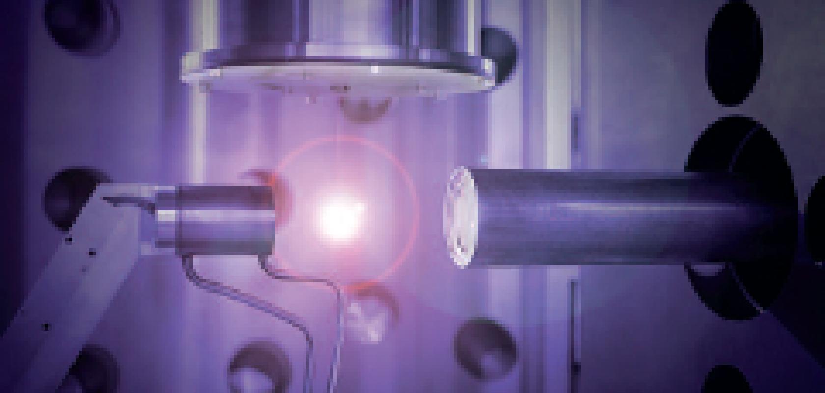
The main method of generating EUV radiation is via laser-produced plasma (LPP) using a high-power CO2 laser of around 20kW to hit tin droplets and form a plasma. This emits radiation, some of which is in the EUV wavelength range of 13.5nm. That radiation is captured and sent into an EUV exposure system through a set of mirrors in a vacuum. All materials absorb EUV, including air, which is why this process has to take place inside a vacuum. The mirrors have EUV reflectivity of close to 70 per cent in order to minimise any light loss.
One of the ways to increase output power is to increase the conversion efficiency, so the amount of EUV radiation gained from the tin droplets. There are about 50,000 of these droplets hit per second. Making sure that each droplet is irradiated by the laser with the maximum conversion efficiency is a good way to increase the power of the system.
Adlyte has said it has demonstrated that its EUV mask inspection technology is now suitable for high volume manufacturing (HVM). ‘The key for inspection is brightness, because the light source is basically a flash,’ explained Abhari. ‘Adlyte meets and exceeds the requirements on brightness. It meets the requirements on power and stability, and we have demonstrated that we meet the requirements on cleanliness over 24 hour operation. This is technology readiness that allows us to move to commercialising this product.’
Adlyte’s EUV sources for mask inspection use similar technology to EUV lithography exposure tools, in that they are LPP light sources. However, mask inspection sources must be smaller, less complex and less expensive compared to a Cymer EUV source, for instance, said Abhari. Also the requirements are different for mask inspection – the customers don’t need as much power for mask inspection, but they need high brightness.
There are different types of mask inspection; there are mask blanks, aerial image measurement system (AIMS), and mask pattern inspection. These are actinic or ‘at wavelength’ inspections and each has slightly different requirements. ‘All have a requirement that the source has to be very clean, such that you don’t put any debris onto the mask,’ explained Abhari.
‘These machines have to run for thousands of hours 24/7,’ he continued. ‘When we talk about HVM readiness, it is mainly to do with serviceability, uptime, spare parts, etc. It is not so much about the science of the technology – that has been demonstrated – but how does that technology integrate with the inspection machine and how do complete systems operate 24/7? This is what we call HVM readiness.’
When tin droplets are irradiated by a high-power pulsed laser it generates debris, neutrons and ions, which has to be managed without imparting any of the debris onto the optics. ‘We have developed, along with the system that generates the stable plasma, layers of debris mitigation, and have demonstrated the system is clean over tens of hours with no debris coming through,’ Abhari stated. ‘This is the state-of-the-art right now and the feasibility studies have been completed; it’s more to do with how to make sure that remains for years of operation. This is the readiness that we are working on right now and also to make sure we have a good understanding of the cost of ownership.’
Adlyte generates tin droplets with a diameter in the range of 30-50µm. These are then fired at high speed at frequencies in excess of 10kHz. The droplets are then tracked in vacuum and are actively positioned to a targeting zone of ±5µm. This triggers a high-power pulsed laser with irradiance that is matched to the tin properties to give the maximum EUV output. The light is extracted through different types of mirrors, including Bragg filters that are multilayer mirrors, which, together with the series of debris mitigation systems, focus the light without any physical barriers. This is one of the key things to avoid debris going through the system. This happens 6,000-10,000 times a second, and it runs continuously in a fully automated manner.
The technology was developed at the ETH Zürich and is under exclusive licence to Adlyte. ‘Now we are working on customised solutions for inspection,’ commented Adlyte. ‘The entire industry is waiting to see when HVM will really start before investing in the next tranche of investments that are needed. The signs from those in the industry, in the last six months, have been positive. We feel the traction and the interest. While we cannot say the exact timing of HVM, we are hopeful that it will not be too far from now.
‘EUV lithography is at a point where readiness has been demonstrated,’ he added. ‘The next stage is more a question of economics as opposed to science and technology, making sure the economics of the system makes sense in a broad supply chain, including inspection.’ l
 Greg Blackman is the editor for Electro Optics, Imaging & Machine Vision Europe, and Laser Systems Europe.
You can contact him at greg.blackman@europascience.com or on +44 (0) 1223 275 472.
Find us on Twitter at @ElectroOptics, @IMVEurope, and @LaserSystemsMag.