The likes of Intel are finding it more difficult to make the smallest features on their silicon chips with current immersion lithography techniques. If microchips keep getting faster at the rate predicted by Gordon Moore, co-founder of Intel, a new means of printing circuits on silicon is needed. Enter extreme UV lithography.
EUV lithography has been hailed for some time as the natural successor to photolithography at 193nm, the established method for printing integrated circuits, because its shorter wavelength of 13.5nm gives a better resolution and the ability to print smaller structures. But it represents a step change. EUV is absorbed by pretty much all material and has to be generated in a vacuum. All the optics have to be reflective. This makes building a reliable and efficient EUV scanner a challenge, unlikely to come to fruition in terms of high-volume chip manufacture for at least a couple of years.
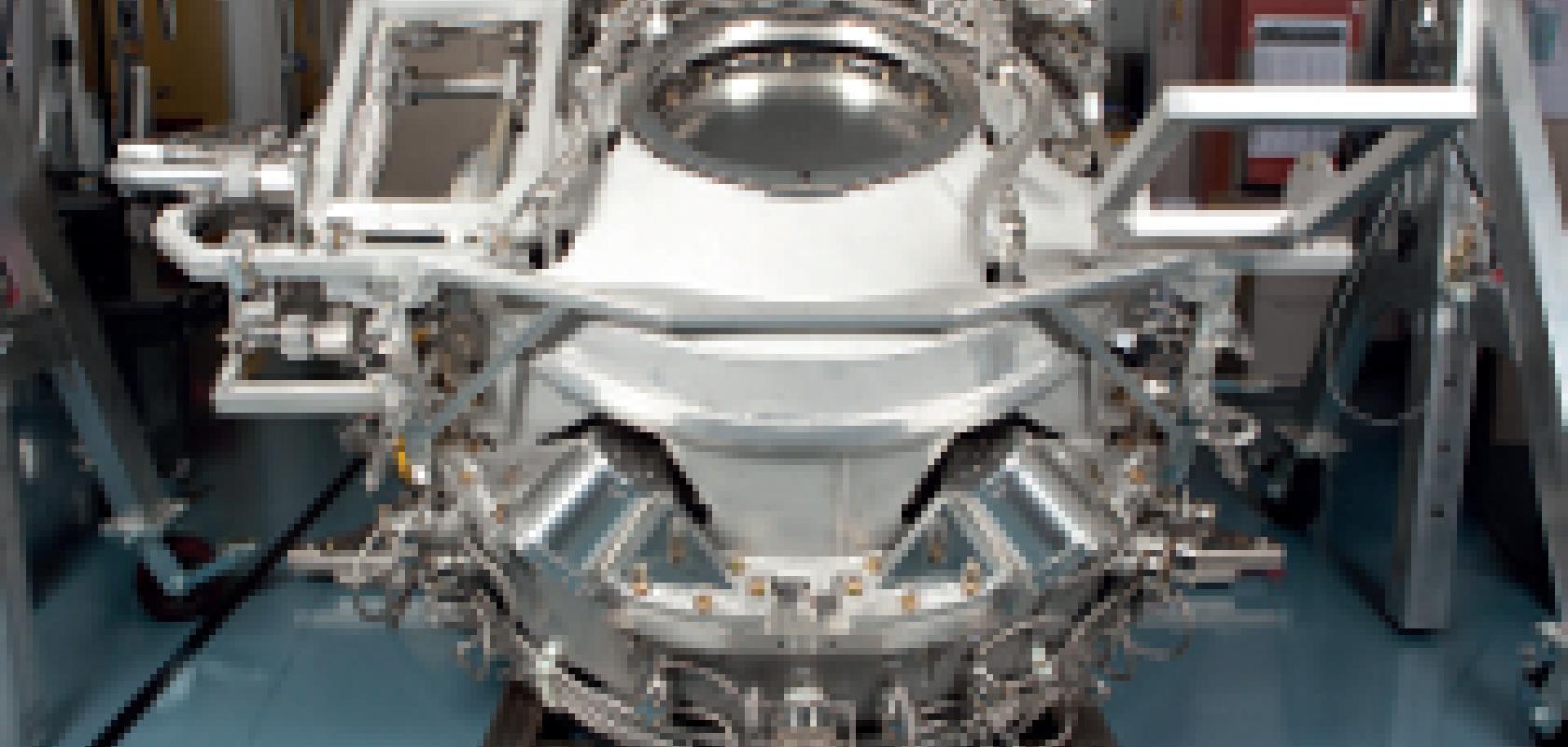
The lithography scanner provider ASML announced in October the purchase of EUV light source maker Cymer to help its EUV programme. EUV pilot production tools from ASML are being tested and the company plans to ship its latest generation of pre-production tools, the NXE:3300B, within a few months. ASML is targeting 11 shipments of the system in 2013, worth around €700 million.
This is all geared towards allowing chip manufacturers to finalise their EUV processes, with production machines expected to be delivering 70 wafers per hour by mid-2014. It won’t be until 2015 or later before chips are being produced by this technology in any kind of volume.
The source of the problem
The EUV light source remains the major stumbling block. Cymer says its current light source operating in the field is running at around 10W of output power; 250W is generally considered the benchmark where EUV scanners become economically viable for silicon chip manufacturers. Cymer’s source has demonstrated 30 to 40W output power, and is currently being integrated into ASML’s scanner. At low duty cycle, Cymer can generate around 90W raw power, but a certain amount of energy overhead is needed to keep a reproducible dose at the wafer.
Cymer bases its EUV source on a laser produced plasma (LPP) architecture, whereby a tin droplet is heated to around 500,000°K with a high-power pulsed CO2 laser. This generates a plasma that emits EUV light at 13.5nm, along with other wavelengths. The EUV radiation is collected with a large mirror coated with silicon molybdenum multilayers, that selects the 13.5nm radiation and focuses it to the intermediate focus, the interface with the scanner.
‘This is really the only architecture scalable to the power levels that will be needed for high-volume manufacturing at high throughput,’ says Dr Nigel Farrar, vice president of EUV strategic marketing at Cymer.
The alternative is discharge produced plasma (DPP), which uses an electrical discharge to generate the plasma, although one problem with the method is its limited scalability to high powers. Xtreme Technologies is developing a hybrid, called laser-assisted discharge plasma (LDP), which it claims combines the advantages of LPP and DPP – power scalability and high stability. The company announced in October 2012 stable operation of its EUV light source over a period of half a year at the Belgian research institute Imec.
Maximising power output
Phil Alibrandi, director of US sales at EUV source provider Gigaphoton, which bases its technology on LPP, says: ‘There are three main areas that can be fine tuned [with LPP] for increased power output: the frequency of the tin droplets supplied to the chamber, the conversion efficiency (CE) of generating EUV energy, and the CO2 drive laser.’
One key technology required for scaling to higher power is a pre-pulse laser, which Cymer and Gigaphoton use. ‘The conversion efficiency without a pre-pulse laser is relatively low because a lot of the drive laser beam misses the droplet,’ says Farrar, the droplet being around 30µm in diameter and the laser beam only focusing down to around 100µm.
The purpose of pre-pulse is to hit the tin droplet with a lower-intensity laser pulse ahead of the main pulse. This increases the size of the droplet so the interaction cross-section with the laser beam is better matched.
Gigaphoton uses a YAG wavelength laser to expand a 20µm diameter tin droplet to around 300µm. It then focuses a 9kW CO2 laser to a spot size of just over 300µm to maximise efficiency. Alibrandi says Gigaphoton’s EUV source has a conversion efficiency of 4.7 per cent, which he says is made possible by using a pre-pulse laser.
However, a pre-pulse laser only gets you so far, and to increase the power output further requires a higher power CO2 drive laser. Gigaphoton calculates a 23kW laser will be needed to reach 250W output power. ‘Ionising each droplet at a rate of 100,000 per second, five per cent conversion efficiency, and a 23kW drive laser should allow 250W output power to be achieved,’ states Alibrandi. The problem, however, with engineering higher power CO2 lasers, involves back-reflection of the laser energy. ‘We’re working to avoid self-oscillation in the laser using filters and pre-amps and increase the [drive laser] power output,’ says Alibrandi. Gigaphoton has begun testing its 25W EUV source, which it will supply to ASML for integration in its scanners.
The collection efficiency – how much EUV light is collected and directed to the intermediate focus – is also important. That depends on the reflectivity and size of the collector mirror, which has to be protected from any tin debris in the chamber. Tin atoms or ions settling on the mirror reduce its reflectivity.
Debris mitigation is a challenge, as more than a few angstroms of tin will render the mirror inoperative. ‘Replacing the mirror is a lengthy and expensive process,’ says Alibrandi. ‘These scanners are $100 million tools and it’s important that they perform.’ Gigaphoton’s debris mitigation mechanism uses superconducting magnets to sweep away excess tin and preserve the lifetime mirror. The company is also developing an on-demand droplet generator, which, it claims, will reduce tin debris inside the chamber.
Cymer claims it can protect its collector mirror up to at least the 40W power levels currently being generated. Cymer has recorded around 2 per cent conversion efficiency with its pre-pulse laser and 4 per cent on solid targets in the lab. ‘The trick is to maintain CE when firing at moving droplets at 50kHz,’ says Farrar. ‘The tin droplets move across the chamber at 30m/s and you have to hit them with two laser beams at about 50,000 times per second. If you don’t hit them dead-on every time, you lose some CE. It’s a different story being able to hit a solid stationary target and being able to hit droplets at this rate. That’s a large part of the challenge.’
Mask technology
Investigations also continue into fabricating better EUV reticles or masks. ‘The system is based on internal reflections between surfaces, one of which is the mask,’ says Kurt Ronse, of Imec, a research institute working on the infrastructure of EUV. ‘That’s not a problem, except that a photomask used in 193nm or 248nm lithography will normally have a pellicle, a thin membrane a few millimetres away from the critical pattern, which keeps particles from falling onto the mask. In EUV you can’t use a fixed pellicle because of the nature of the radiation.’
Defects will be replicated throughout every die and every wafer printed with that mask, so it’s important to keep them to a minimum. One method being investigated is using dual pods, where an inner pod serves as a pellicle. The inner pot is removed during the exposure and then mounted again until the next exposure, so there’s always a short period where the mask is unprotected. Defects can also be introduced during fabrication and defects a few nanometres thick can create printing errors.
Another critical issue lies in the processing and the resist chemistry of EUV lithography, in the sense that it’s difficult to reach the resolutions EUV promises (EUV is currently targeted at sub-20nm feature sizes). This will have to advance before EUV can become a commercial technology.
Chip makers need EUV lithography
The goal for EUV sources is 250W of power, but chip manufacturers can use EUV scanners and derive big benefits at lower power. Eric Meurice, CEO of ASML, said that once EUV proves itself at a throughput of 60 wafers per hour it will replace immersion lithography in the critical layers at the 14nm node.
The resolution capability of these EUV scanners is so much better than immersion lithography because of the shorter wavelength. This means that, for a particular process layer, fewer masks are needed – a significant cost saving.
‘The industry, the memory and logic chip manufacturers, are screaming out for EUV to become available as soon as possible,’ Ronse says. ‘Up until now, chip manufacturers have been able to fabricate smaller features with multiple patterning. This works down to the 20nm logic technology node, but moving to the 14nm node would mean a lot of the layers would require triple patterning, in some cases quadruple patterning. This requires so many lithography steps, deposition steps, and etch steps that the process becomes too complex. The industry would probably rather wait for EUV to become available for the 14nm node.’
Manufacturers are trying to make 193nm multiple patterning techniques more cost-effective, says Ronse, by relaxing some design rules and imposing more design restrictions while EUV gets up to speed. Even so, high-volume production won’t be in place until 2015 at the earliest, say most commentators – but, as Meurice said, once commercially available, EUV will provide scaling capabilities, i.e. shrinking feature sizes, that could last another 10 or 15 years.
 Greg Blackman is the editor for Electro Optics, Imaging & Machine Vision Europe, and Laser Systems Europe.
You can contact him at greg.blackman@europascience.com or on +44 (0) 1223 275 472.
Find us on Twitter at @ElectroOptics, @IMVEurope, and @LaserSystemsMag.