When it comes to the next big display technology, all eyes are on microLEDs. Promising stunning picture quality with spectacularly high resolution and brightness, tech companies far and wide are muscling in on the diminutive yet mighty flat-panel starlet.
Earlier this year, industry behemoth, Samsung, unveiled its latest raft of 110-inch, 101-inch and 89-inch displays, while LG is poised to push picture boundaries with a 100-inch plus microLED display. Meanwhile, Apple, Meta and other multinationals continue to hone their display-tech behind closed doors, as start-ups such as PlayNitride and Plessey serve up microLED innovation. And, with many industry analysts predicting market growth to top 100 per cent in the coming years, the industry frenzy is understandable.
Eric Virey, technology analyst at France-based Yole Développement, has been tracking microLED developments for some time while keeping a close eye on microLED patents and who’s been filing these all-important indicators of industry progress. As he pointed out: ‘The level of activity here is still increasing exponentially... and what we can see now is a trend towards more mature patents.’
According to Virey, a few years ago the patents were generally about ideas or concepts, but not anymore. ‘We’re now seeing a great deal of detail on describing precisely the structure of the pixels, the nature of the materials and how this is all put together,’ he said. ‘You can tell that many of the companies filing these patents are actually in the fab, trying to make [the technology] work.’
The patent landscape moved up a gear in 2014, when Apple acquired lower power microLED start-up LuxVue. Suddenly, more display manufacturers and OEMs started to take the technology more seriously – be it for augmented reality or large-screen TV applications – and today, patents on microLED chips, including novel die structures, are flying in from everywhere. China-based organisations, such as China Start Optoelectronics Technology, are now also generating vast swathes of intellectual property.
Along the way, industry acquisitions and strategic investments have been rife, generating even more market excitement. For example, Facebook, now Meta, has been building microLED IP for AR and VR applications, buying Oculus, microLED start-ups, InfiniLED, mLED, and gaining full exclusivity to Plessey’s microLED technology and manufacturing capacity. At the same time, Samsung has invested in numerous start-ups, most notably Taiwan’s PlayNitride.
‘We’re seeing the technology coming into place, the supply chain coming into place and prototype demonstrations are increasingly convincing,’ Virey remarked. ‘As I like to say, we’ve finally reached escape velocity.’
Industry hurdles
Still, to move from escape velocity to a steady acceleration, the microLED display industry must first face numerous sticking points, most notably, mass transfer. The manufacture of any microLED display involves making microLEDs – with diameters ranging from 5µm to 100µm – and using millions and millions of these devices to form the self-emitting sub-pixels within a display. During a traditional pick-and-place transfer process, the microLED display would be assembled one sub-pixel at a time onto the display backplane, which given the sheer numbers of devices is extraordinarily time-consuming and expensive. What’s more, many pick-and-place processes struggle to handle pixel diameters of less than 50µm.
- MicroLED startups 'challenge heavyweights'
- MicroLED chips on 300mm silicon wafers pave way for mass production
- MicroLEDs key to enhancing AR - from Photonics West 2020
Given these issues, microLED display players have been devising alternative mass transfer processes, typically using elastomer stamps or lasers to lift thousands of microLED chips from the source wafer to the display panel in a single swoop. For example, US-based X-Display pioneered the use of elastomer stamps more than a decade ago, while Toray Engineering of Japan has since been manufacturing both stamp- and laser-based mass transfer tools. Over in Germany, photonics firm, Coherent, has been collaborating with laser equipment manufacturer, 3D Micromac, which recently launched MicroCeti, said to transfer more than 130 million microLEDs an hour. Also, ASM Pacific Technology, TDK in Japan, Smart Equipment Technology in France, and more, have released or are about to deliver mass transfer tools.
‘There’s definitely been a shift in how the technology is evolving,’ Virey said. ‘Not long ago there were no mass transfer tools available but this has changed significantly in the last 12 to 18 months – we’re seeing a lot of reputable equipment makers jumping into the field.’
He added: ‘In some cases, such as Toray Engineering, companies are coming up with a full suite of tools that not only include mass transfer but also inspection and repair. So I think we’re heading to a situation where you will be able to buy almost a turnkey solution.’
And while most organisations keep their transfer yields under wraps, industry reports suggest figures are edging closer towards the much-coveted 99.9999 per cent deemed desirable for cost-effective mass production. ‘We’re not there yet but mass transfer is no longer seen as that major roadblock that could completely derail microLEDs,’ Virey said.
But while the industry focus appears to rest on either stamp or laser-assisted mass transfer, other innovative approaches are moving forward rapidly. One such example is fluidic self-assembly, a massively parallel process developed by US-based eLux, which spun out of Sharp Laboratories of America in 2016.
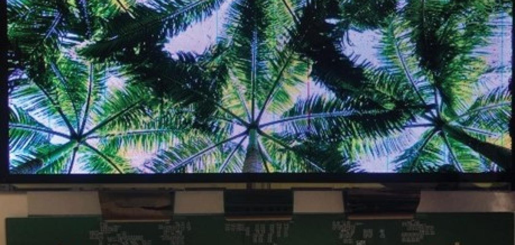
MicroLED display with 42 pixels per inch made by fluidic assembly from eLux. Credit: eLux
The production process begins by first mapping defects on the microLED wafer. Here, eLux uses optical inspection, micro-photoluminescence and cathodoluminescence to detect defective microLEDs on the wafer, ensuring that they only harvest the ‘good’ devices for a display. Millions of these microLEDs are then held in a liquid suspension and repeatedly passed backwards and forwards across a substrate or backplane, populated with wells. Critically, these wells are arranged as the display pixels and trap the microLEDs as they settle to the bottom of the suspension.
As eLux chief technology officer, Paul Schuele, noted, largely thanks to its initial wafer-mapping production step, yields are good, with the technology lending itself to the creation of the microLED tiles destined for use in the massive displays from the likes of Samsung and LG. ‘Our natural advantages head towards television,’ he said.
Indeed, in Spring last year, the company demonstrated a 12.3-inch display tile that comprised 518,400 microLEDs and was assembled in just ten minutes – equal to an assembly rate of 3.1 million microLEDs per hour – with a yield of 99.987 per cent. Given a 4K television has 8.3 million pixels, Schuele and colleagues reckon their results are approaching the quality required for a commercial microLED television. Right now, eLux is working on its latest microLED-based zero bezel width tile architecture with Taiwan-based investor and TFT LCD panel manufacturer, Innolux, that can be tiled to any size. Elux has also set up an automated fluidic assembly tool in its prototype lab, in Taiwan, assembling panels up to 15-inch diagonal.
‘You know, our R&D tool is really cheap; it costs about $13,000 while a good pick-and-place tool can be more than a million dollars,’ pointed out Schuele. ‘And of course if you are making a really big display then the process of pick-and-place is just going to get more expensive.’
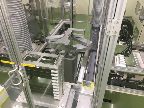
Elux’s fully automatic cassette-to-cassette fluidic assembly of ten display panels up to 15-inch diagonal. Credit: eLux
Still, as Schuele also noted, the jury is out on which microLED assembly method industry will favour, with each having different trade-offs. ‘Right now, it looks like pick-and-place has fallen back for a whole bunch of reasons and laser-based transfer is perhaps dominant, but I don’t think it’s clear what the ultimate winning technology will be,’ he said. ‘Everybody’s learning at this point and, ultimately, I think there is going to be some kind of combination of all this learning because the desirability of the big microLED display is hard to argue against... but ultimately one has to win.’
A different tack
Another start-up doing things differently is France-based Aledia. While most industry players form microLED structures by depositing 2D planar gallium nitride semiconductor layers on relatively small 100mm and 150mm sapphire substrates, the CEA-Leti spin-off grows GaN nanowires directly onto 200mm and 300mm silicon wafers.
The key benefits for Aledia are two-fold. Firstly, growing nanowires on silicon prevents the accumulation of the wafer defect-inducing stresses that arise when GaN layers are deposited on silicon or sapphire. Secondly, fabricating devices directly onto silicon wafers means the company will eventually reap the economies of scale that can only come from using silicon foundries.
On top of this, Aledia also claims to have developed a parallel mass transfer method to shift millions of nanowires from the silicon wafer to the display backplane. Aledia chief executive, Giorgio Anania, remains tight-lipped on his company’s approach, but said: ‘Our nanowires are perfect crystals – bad nanowires are very rare. We also have about 20 nanowires on a sub-pixel... and can transfer 100 per cent [of these nanowires]. This completely changes your transfer approach and means you can do things that you couldn’t do before.’
He continued: ‘Yields are going up on other transfer approaches but I just don’t know what their costs are going to be. However, many start-ups are developing technology here... and equipment companies are coming up with new [methods] that will transfer more chips, and faster – the whole ecosystem is awake.’
Aledia has already attracted more than €100 million of investment from myriad investors including several large technology companies, semiconductor equipment manufacturer, Tokyo Electron, and Intel Capital. And product-wise, the company has its sights set on many market segments from smartwatches and virtual and augmented reality displays, to laptops and televisions. The first low-volume offering is scheduled to leave Aledia’s pilot line later this year with high-volume production set to start in 2024 once the company’s large-scale, France-based manufacturing facility is up and running.
‘Our first products are probably going to be larger – we’re starting big and going medium then small,’ Anania said. ‘I think we cracked most of our problems last year and now we need to deliver – but you can assume that we’re attacking all the major market segments.’
So as businesses, from start-up to tech-giant, gear up to launch a glittering array of microLED products and displays, what can the world expect next? Focusing on microLED televisions, eLux’s Scheule highlighted how industry players are acting fast, with investments rising and prices also coming down. Indeed, he’s now looking forward to the Costco mass market moment.
‘When will we see a microLED television in Costco?’ he asked. ‘I would say it’s probably three years out, but could be as much as five years – I’d be shocked if we see this in less than two years, but also shocked if it was more than five years.’
Elux has demonstrated fluidic assembly of three size microLEDs (50µm, 40µm and 30µm) to make a native RGB display. Credit: eLux
At CES 2022 in Las Vegas, Yole’s Virey was impressed with the latest Samsung TV: ‘I couldn’t see the seams and the connection between the different tiles, and the image quality was really outstanding.’
However, Virey also pointed to the promise of augmented reality smart glasses, citing the latest offering from US-based Vuzix. ‘This is their first commercial product using a microLED display and it’s the most convincing experience I’ve had with smart glasses. It’s a monochrome green display yet it’s so bright, clear and crisp – there’s no haze and no defects – the image is physically floating about an arm’s length in front of you.’
Given these developments, Virey expects to see professional enterprise applications first, delivered by the likes of Vuzix’s smart glasses, with full-colour, high-volume consumer AR products following in the next few years. China-based Jade Bird Displays also claims to have sold a million microLED displays last year, targeting smart glasses. ‘I’m the most optimistic for augmented reality applications, but for other applications, there is the question mark of cost,’ he said. ‘All the technology breaks are coming into place, the supply chain is coming into place, but there’s still this issue of cost. The biggest cost contributor is the microLED die itself and the second major obstacle is overall yield management,’ he added. ‘But get those two things right, and you’re getting closer to a product.’
Sponsored content
Display colour measurements – getting it right without compromise
The consumer electronics industry is a multi-billion-dollar market, with the latest figures from data firm, Statista, predicting a worldwide spend of around $2.06tn by 2023 on consumer electronics devices.
To offer an example, according to independent research firm, Strategy Analytics, almost half of the global population now owns a smartphone. This is without taking into account televisions, AR and VR technology, wearables, voice technology and other consumer products.
In such a busy and competitive market, with new players entering at pace, it is essential for manufacturers to be able to operate at maximum efficiency, both to meet demand and to ensure quality levels are of the same high standard in every product produced.
This is certainly the case when it comes to the displays for these products, as Steven Goetstouwers, CEO at Admesy, has witnessed over the last 15 years through the company’s work with some of the leading consumer electronics manufacturers. ‘It is important that all consumer devices sold in a shop look the same, according to brand, to the end customer,’ he explained. ‘There should be nothing obvious, such as, for example, a display having a yellow tone when it should be white.’
Repeatability as standard
To ensure this is the case, manufacturers require incredibly accurate and yet very fast colour measuring equipment. ‘It has to be accurate, because the human eye is extremely adept at spotting colour differences,’ said Goetstouwers. ‘It has to be fast, because with consumer electronics applications, they’re not building one device, they’re building tens of millions.’
One particular application led to Admesy collaborating with a customer to provide a particular colorimeter. ‘Manufacturers are now putting items underneath the display,’ explained Goetstouwers. ‘For instance, they are building fingerprint scanners, cameras or facial recognition under the display, to produce a phone, tablet or a laptop without a border or a cut-out for a camera. But this can weaken the part of the display with the item underneath it.’
This means there is a potential spot where the performance of a display might differ, and this particular customer had the requirement to measure this point to ensure this particular part of the display had the same performance as the rest of the display.
‘The challenge,’ continued Goetstouwers, ‘is that it had to be small, and to go small, you have to start with an extremely fast colour measurement.’ This is due to the risk that a smaller size could reduce the measurement speed. ‘You need a very fast device to start with,’ he explained, ‘because you know you could lose a lot of speed by focusing-in, and you need a very complex lens system to still get a relatively fast sampling speed. We also ran into a very interesting, practical aspect: at this size, how do you still know that you’re looking at the right spot?’
To compare, traditionally the measured spots in a display would be 10 or 20mm and they would be in the centre, which would allow for a certain margin of error. ‘Now,’ said Goetstouwers, ‘because it’s such a small spot, if you miss a line, even only briefly, the measurement spot and the spot size don’t align well and the illuminance values could be incorrect.’
The solution
This was solved by putting in an alignment light in the centre of the measurement spot, so instead of only measuring, the colorimeter can also send a red LED dot, which can be used to check with the camera to ensure it is where it is supposed to be. ‘That information can be used to ensure the holes are aligned properly,’ revealed Goetstouwers.
The team at Admesy also noticed that other customers were experiencing similar requirements. ‘We basically went from providing just the sensor and measurement tool, to more of a full system because now there is an alignment tool included, and if the data is read correctly, the positioning of the display or the measurement can be adjusted based on that information.’
The result of the project is the Prometheus series of colorimeters, which is now available to all customers, thanks to a lot of hard work and cooperation between Admesy’s optical and mechanical engineers. ‘This whole lens design is one of the more complex ones we have done,’ said Goetstouwers. ‘And the engineers were able to build it in such a way that it is scalable using a normal production process.’
The Prometheus series includes flicker and response time measurement options to the colour measurements and offers a larger dynamic range and increased sampling speed than its predecessor, the Hyperion colorimeter. It is also designed to be robust for 24/7 use, and easy to integrate in production environments. A number of different lenses are available. For general display measurements there are collimating lenses with 10, 20 or 27mm spot size. For smaller areas of interest, or special applications like those detailed in this case study, a focusing lens version with 2.1 or 5mm spot size is also an option.
Further information: www.admesy.com/en/series/prometheus/