
To increase the processing speed and reduce the power consumption of electronic devices, the microelectronics industry continues to push for smaller and smaller feature sizes. Transistors in today's cell phones are typically 10nm across or smaller. Scaling transistors down below these dimensions with higher accuracy requires advanced processes for lithography, the primary technique for printing electrical circuit elements on silicon wafers to manufacture electronic chips.
New research suggests that metalenses could play a role in advancing lithographic processes and, ultimately, making chips. Mao Ye and researchers at the University of Michigan have developed metalenses that focus light into a pre-designed pattern rather than to a point, which suggests they could be used to carve circuits into silicon.
While a traditional lens is made from glass, metalenses use flat surfaces made up of nanostructures to focus light. These simple, flat surface lenses could replace bulky, curved lenses currently used in optical devices. Recent advances in metasurfaces provide a new basis for recasting optical components into thin, planar elements, having similar or better performance using arrays of subwavelength-spaced optical phase-shifters.
In 2017, researchers Alan She and colleagues at Harvard University produced metalenses through the process of photolithography, which carves sub-wavelength features onto flat sheets of glass. They were able to arrange these features in ways that scatter light with greater control than what was possible before – the resulting metalenses, the researchers promised, were set to revolutionise consumer electronics and computing.
The major advantage of metalenses is that they can be produced on the same fabrication lines as silicon chips, rather than made separately and then assembled into optical components as per traditional lenses. This could allow optical elements inside consumer devices – such as cameras in smartphones – to be made much more cost effectively. It could also enable new possibilities for photonic integrated circuits (PICs).
Ye and colleagues at the University of Michigan demonstrated metalenses that can focus light into a designed pattern rather than to a point. This would benefit chip makers who use photolithography to produce specific patterns onto the surface of a silicon slab.
A metalens typically consists of a particular pattern of channels, which focuses light to a specific focal point. To create a pattern, the research team added another pattern with a slightly different focal point that overlaps the first, which creates a focal line. In principle, any pattern can be created by adding more patterns with different overlapping focal points.
To demonstrate this principle, the researchers produced two lenses with different patterns – one with an ‘M’-shaped focus and one with a ‘U’. According to the team, this shows how complex patterns can be created using the overlaying technique.
‘Due to the large energy density that concentrates on the pattern, metalenses of this kind can potentially be applied to next generation nano-lithography with targeted pattern imprinted on the lens,’ the researchers said. The technique also has applications that involve beam engineering, they add: ‘A wide range of patterns can be generated by combination of basic elements, such as “point”, “line” and “curve” that bring extra degrees of flexibility to beam shaping.'
Scaling up metalenses
The University of Michigan’s research suggests metalenses could advance lithography in chip making. But lithography is also a key technique used to make metalenses.
Researchers at Harvard University have developed a centimetre-scale metalens that can be scaled up – pushing it closer to being produced on chip fabrication lines and added to consumer electronic devices.
It is the first mass-producible, all-glass, centimetre-scale metalens in the visible spectrum.
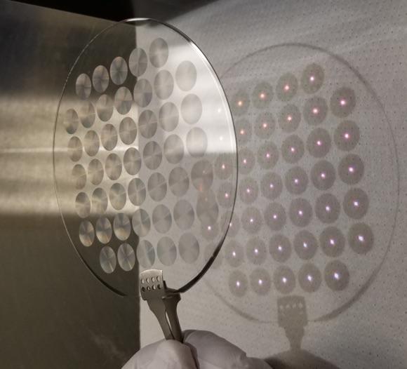
Forty-five 1cm metalenses on a silicon wafer focus light on a sheet of paper. Credit: Joon-Suh Park/Harvard SEAS
According to the researchers at the Harvard John A Paulson School of Engineering and Applied Sciences (SEAS), most of metalenses developed until now are about the size of a piece of glitter. While lenses this size work well for some applications, a larger lens is needed for low-light conditions, such as an imaging system onboard orbital satellites, and VR applications, where the lens needs to be larger than a pupil.
Larger-sized metalenses have been difficult to mass produce before, but the team have now succeeded using deep-ultraviolet (DUV) projection lithography.
The team's metalens was described in a paper published in Nano Letters in November 2019.
‘This research paves the way for so-called wafer level cameras for cell phones, where the CMOS chip and the metalenses can be directly stacked on top of each other with easy optical alignment because they are both flat,’ said Federico Capasso, senior research Fellow at SEAS and senior author of the paper. ‘In the future, the same company can make both the chip and the lenses because both can be made using the same technology: lithography.’
Joon-Suh Park, PhD student and first author of the paper, added: ‘Previously, we were not able to achieve mass-production of centimetre-scale metalenses at visible wavelengths because we were either using electron-beam lithography, which is too time consuming, or a technique called i-line stepper lithography, which does not have enough resolution to pattern the required subwavelength-sized structures.'
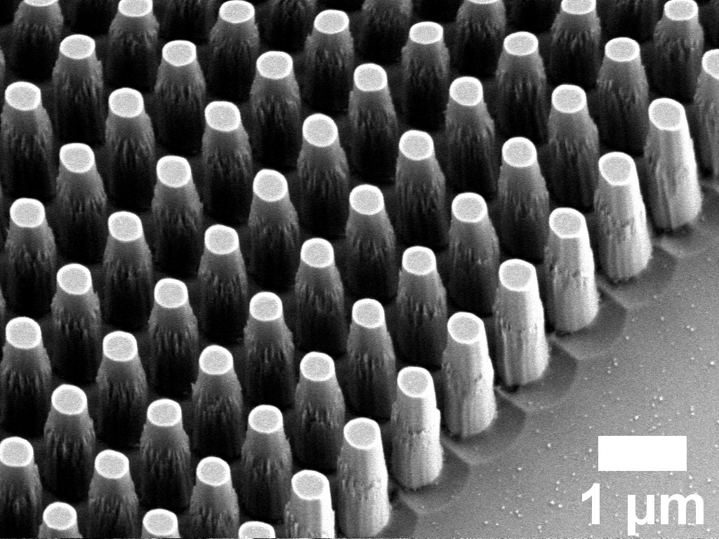
Zoom-in SEM image of nanopillars of the metalens. Credit: Joon-Suh Park/Harvard SEAS
To mass produce a centimeter-scale metalens, the researchers used a technique called deep-ultraviolet (DUV) projection lithography, which is commonly used to pattern very fine lines and shapes in silicon chips in everything from computers to cell phones. The technique can produce many metalenses per chip, each made of millions of nanoscale elements with a single shot of exposure, like taking a photograph.
DUV projection lithography is commonly used to pattern very fine lines and shapes in silicon chips in everything from computers to cell phones. The technique can produce many metalenses per chip, each made of millions of nanoscale elements with a single shot of exposure, like taking a photograph.
The researchers eliminated the time-consuming deposition processes that were required for previous metalenses by etching the nanostructure pattern directly onto a glass surface.
While this lens is chromatic, meaning all the different colours of light do not focus at the same spot, the researchers are working on large-diameter achromatic metalenses.
A European research consortium is developing a lithography method that could permit the 3D printing of organs.
The Horizon 2020 project has been granted just under €3.5m over three years (2019-2022). Called ‘Brighter’ (standing for ‘Bioprinting by light sheet lithography: engineering complex tissues with high resolution at high speed’), the project is being coordinated by Dr Elena Martinez (IBEC, Barcelona) and involves the Goethe University Frankfurt.
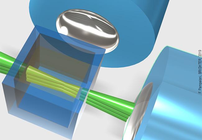
A hydrogel composed of living cells and photosensitive molecules is deposited in a special cuvette. A thin laser light sheet illuminates the gel following a programmed pattern (green beam). This leads to the formation of 3D micro-structures that reproduce the tissue architecture and function. The remaining, still liquid hydrogel is washed out after the printing process. Credit: F Pampaloni, Brighter project, 2019
The production of artificial organs is a hot research topic. In the near future, artificial organs will compensate for the lack of organ donations and replace animal experiments. Although there are already promising experiments with 3D printers that use a ‘bio-ink’ containing living cells, a functional organ has never been created in this way.
The H2020 consortium is developing a lithography method that relies on light sheet illumination and on special photosensitive hydrogels that are mixed with living cells.
Bio-printing systems that build up structures layer by layer (bottom-up approach) have considerable disadvantages. On the one hand, the printing process takes far too long, so that the survival chances of the cells in the bio-ink and in the polymerised layers decrease. Furthermore, the extrusion pressure leads to a considerable cell death rate, especially for stem cells. In addition, the resolution of the method, around 300 micrometres, is far too low to reproduce the delicate structures of natural tissue. Finally, it is particularly difficult to integrate complex hollow structures, e.g. blood vessels, into the cell tissue.
‘With our project, we want to go the other way round by developing a top-down lithography method,’ explained Dr Francesco Pampaloni from the Buchmann Institute for Molecular Life Sciences (BMLS) at Goethe University. The process works in a similar way to lithography in semiconductor technology. Instead of the semiconductor and the photosensitive layer, which is illuminated by a mask, a hydrogel with photosensitive molecules is used. This is exposed to a thin laser light sheet using the technique invented by Professor Ernst Stelzer for light sheet microscopy. This leads to the formation of branched chain structures (polymers) that serve as a matrix for colonisation by living cells. The remaining, still liquid hydrogel is washed out.
‘This method will enable us to adjust the spatial structure and the stiffness with an unprecedented resolution so that we can create the same heterogeneous microstructures that cells find in natural tissues,’ explained Pampaloni.
Pampaloni expects that completely new possibilities will emerge for the bio-fabrication of complex tissues and their anatomical microstructures. In addition, the specific properties of the matrix can be used to introduce stem cells into well-defined compartments or to enable the formation of vessels. Further advantages over conventional 3D printing systems are high speed and cost-effective production.
Further partners of the project include the IBEC (Barcelona, Spain, coordination), Technion (Haifa, Israel) and the companies Cellendes (Reutlingen, Germany) and Mycronic (Täby, Sweden).