For decades, the standard method of measuring the surface quality of optical components has relied on visual inspection and human judgement. Although this may be adequate, many have scrutinised the approach for not being quantitative enough for performance-based specifications.
There has been pressure to replace subjective inspections with objective tests that can be documented in order to reduce incoming rejection rates, prevent disruption to work flow, and improve customer-supplier relationships.
Thanks to a new tool launched by RedLux in October, which the company says is the industry’s first device for measuring surface quality repeatedly, the manner of verifying optics could be about to change.
Scratch-dig
The surface quality of an optical component refers to the level of imperfections that can be seen visually on its surface, which may have been caused during manufacturing or handling the optic. In the majority of cases, these defects have little to no adverse effect on overall system performance, causing only slight increases in scattered light and minor reductions in throughput.
However, certain surfaces are more sensitive to these imperfections. For example, a defect on a surface located at an image plane can degrade overall image quality, whereas defects on surfaces exposed to high-power radiation can result in increased absorption of energy and may damage the optic.
The US Military Performance Specification, MIL-PRF-13830B, has become the standard method for rating surface quality. The standard sets guidelines for the amount of area surface defects occupy relative to the overall clear aperture of the optical element. Assessments are made relative to the size of the optical component; so, a scratch that is unacceptable for a small part may be adequate for a large part.
Digitising the scratch-dig inspection process
Although the optics industry demands the greatest accuracy, the go-to approach for inspecting optics for scratches and digs has, up until now, relied on human judgement, making it difficult to obtain repeatable results.
Typically, the method involves holding the optic under inspection at a specific angle under specific light conditions – as defined by the standard – and the user will compare the optic to a set of criteria.
‘For the last 65 to 70 years, the optics industry has relied on looking at their optics to determine whether or not they can see a scratch or a mark on the surface such that they can pass or fail that optic during quality control,’ explained Mike Hobby, sales director at RedLux.
This subjective and often undocumented scratch-dig inspection process all too often leads to discrepancies in the supply chain, which can increase production costs, added Hobby: ‘The manufacturer sends the inspected optics to the customer, who then checks them in the same manner, and the argument begins – the customer thinks they can see a scratch, sends the goods back, the manufacturer re-inspects them and cannot see a scratch, and so on. It’s a nightmare,’ said Hobby.
‘The optics industry is thwarted by manufacturers shipping goods to customers under a subjective quality control, against a set of standards that somebody basically looks at and makes a judgement call on,’ Hobby remarked.
At the Photonex trade show that took place in Coventry, UK in October, RedLux launched a new product to allow optics manufacturers and their customers control their scratch-dig inspection process.
The OptiLux SD uses a dark field camera to certify a component’s compliance to the MIL-13830B specification in a repeatable and traceable fashion.
‘We have, for the first time in the industry’s history, a way of repeatedly measuring [for scratches and digs] such that there is no subjective judgement call on the quality of that optic,’ explained Hobby.
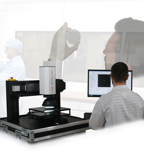
Redlux's OptiLux SD can be used to obtain repeatable scratch-dig measurements
Aligning manufacturer and customer
Crystran, a manufacturer of optical components, has been using RedLux’s device to measure its high-value 190 x 130 x 4mm zinc selenide (ZnSe) windows since 2015. Zinc selenide is widely used for infrared components such as thermal imaging windows and lenses.
These components are anti-reflection (AR) coated after polishing, and this process makes up 40 per cent of the total production cost. So, the manufacturer must be confident that the surface quality is within specification both before and after coating takes place.
By adopting an OptiLux SD machine, Crystran has been able to ship high-value components, such as its ZnSe windows, with a traceable pass/fail MIL-13830B compliant report, therefore avoiding the costs associated with scratch-dig subjectivity within the supply chain.
‘Crystran can now provide direct assurance to their customers that their optical products have been assessed in exact accordance with MIL-13830B, by way of a detailed surface quality report. In addition to reducing the amount of manufacturing re-work and polishing effort Crystran’s customers can be confident that even the most stringent S-D specification has been met,’ commented Hobby.
‘We’ve been able to align supplier, customer and contractor’s expectations of optic quality so that everyone can sing off the same song sheet. It will make the optics industry far more efficient in how it can quality control these flat optics,’ Hobby added.
In addition to automating the scratch-dig inspection process, the OptiLux SD limits the amount of component handling, minimising the potential of accidental damage on soft material such as ZnSe.
Furthermore, the OptiLux SD allows technicians to understand how close an imperfection is to the grading boundary, allowing them to refine their production process by knowing exactly when to stop and when to continue polishing in order to meet the surface specification.
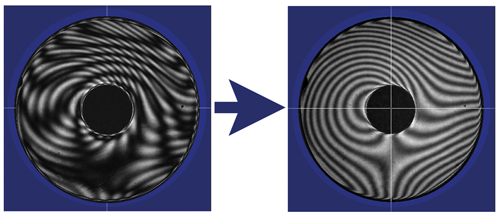
Fringes on a plane-parallel glass disk without the use of 4D's surface isolation source (left) and with (right)
High-resolution metrology
Although checking optics for scratches and digs has only become automated recently, the tools for analysing other optical properties are well-established and can be used to measure with sub-nanometre resolution.
‘The envelope has been pushed over the last few years with the development of very high resolution interferometers,’ said Tyler Steele, product manager for laser interferometers at Zygo.
‘Over the last several years what is becoming more important is very high performance in the high end – so the end application being a high-end imaging system, or a lithography system where it is very important to get light through the optical system and to a very specific point,’ said Steele. ‘To measure components in a very high-precision optical system requires a high-resolution interferometer, more specifically with a very high lateral resolution.’
Put simply, interferometers work by shining laser light onto a test optic, which is then reflected back into the interferometer and compared to light from a perfect reference. ‘Since you’re comparing through a near-perfect reference, the test light will show some amount of deviation, and that deviation is what you’re specifying,’ explained Steele. ‘So, if I have a specification on an optic which needs to be a quarter of a wavelength of surface form, an interferometer will tell me directly what the form error is from a perfect reference.’
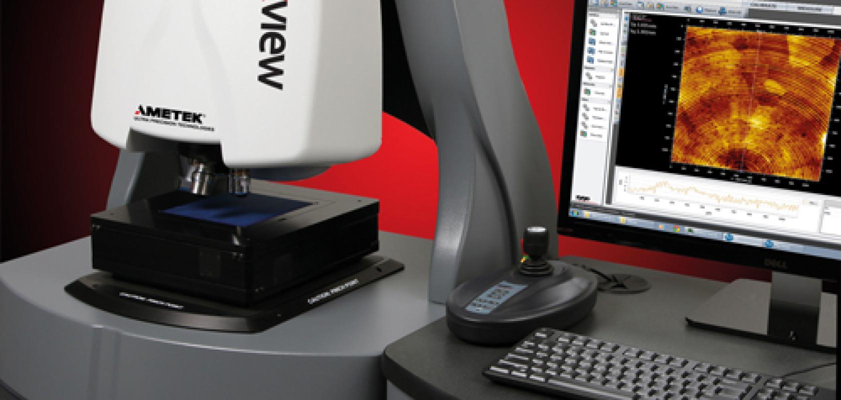
Zygo’s Nexview 3D optical profiler enables quantitative areal topography of thin films (≥50nm thick) without contact or preparation. It can measure full area film thickness and topography, substrate topography and thickness variation maps simultaneously, as well as true corrected surface maps of dissimilar materials.
As optical systems become ever more complex in the future, resolution will continue to improve, noted Steele. ‘Resolution will continue to increase as we bridge the gap between macroscale form errors down to medium-scale waviness down to micro waviness and then to the microscope regime,’ Steele remarked. ‘Certainly interferometry system performance will need to improve along with that.’
Being able to collect high-precision data in a reliable manner will be important as resolutions continue to increase, added Steele, and software for ease of use and for achieving the desired type of analysis after acquiring high-precision data will also need to improve. Lastly, ‘being able to qualify an interferometer – to show that it is indeed achieving the performance that is required – is something we’ll be pushing,’ said Steele.
In some cases, however, there can challenges associated with verifying optics using an interferometer. For example, the difficulty associated with measuring plane-parallel optics – transparent components with parallel faces or systems with two or more parallel surfaces – is that all of the surfaces in the optical path will interfere, making measurement difficult or impossible.
‘The typical approach is to isolate one surface to measure at a time, typically by coating all other surfaces. It is a messy and time-consuming process and can lead to part damage,’ said Mike Zecchino, marketing communications manager at 4D Technology.
A new surface isolation source (SIS) has been developed that allows an operator to isolate optically each surface of a plane-parallel optic for measurement. 4D’s AccuFiz SIS is an optional, external laser source that excludes all but the surface of interest. Both surfaces of a transparent optic can then be measured, and transmitted wavefront error, optical thickness and homogeneity can be calculated. The company will be exhibiting the product during the Photonics West trade show, to be held in January 2017 in San Francisco.
Further information
4D Technology
Redlux
Zygo