Skip to main content
Social media links EO
LinkedIn
Twitter
Log in
Register
Applications
Life sciences
Environment
Quantum
Defence
Automotive
Aerospace
Medical engineering
Electronics
Optical communication
Technologies
Illumination & energy
Imaging
Industrial lasers
Lasers & optoelectronics
Sensors, test & measurement
Photonics 100
UK Photonics
Photonics Frontiers
Resources
Webcasts
White Papers
Supplier
Events
Products
Search
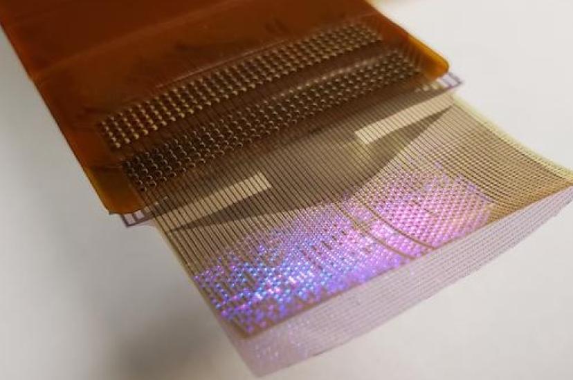
Dual-sided chip combines photonic/electronic functions simultaneously
Morphotonics raises $10m for scalable display optics production tech
ams Osram microLED exit plan leads to job and cost losses
MicroLED display monitors brain activity in real time for more precise surgery
ams Osram stock plummets 40% due to cancellation of 'cornerstone' microLED project
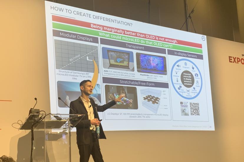
Photonics West 2024: MicroLED commercialisation must accelerate to compete with OLEDs
New partnerships to advance microLED displays
Electro Optics November is out now!
Why AR/VR developers must close the microLED 'efficiency gap'
Ams Osram receives €300m for optoelectronics semiconductor innovation
Pagination
Previous page
‹‹
Page 2
Next page
››
Media Partners

")