An Oxford-based silicon photonics startup has raised $11.5 million to develop a high-speed multi-chip processor combining photonics and electronics to accelerate exponential advances in AI.
Salience Labs was spun-out of the University of Oxford and the University of Münster in 2021 to commercialise an ultra high-speed multi-chip processor that packages a photonics chip together with standard electronics. The technology is highly scalable, capable of stacking up to 64 vectors into a beam of light. By using a broad bandwidth of light to execute operations, Salience Labs delivers massively parallel processing performance within a given power envelope.
Jalal Bagherli, Salience Labs investor and former CEO of Dialog Semiconductor said: ‘The team at Salience Labs is world-class, combining commercial and technical acumen with a disruptive market vision. Their unique ‘on-memory compute’ architecture is ground-breaking, with the potential for breakthrough performance and power capability beyond what the established CMOS roadmap offers.’
The round was led by Cambridge Innovation Capital and Oxford Science Enterprises, with Oxford Investment Consultants, former CEO of Dialog Semiconductor Jalal Bagherli, Silicon Catalyst, the Goh Family Office from Singapore and Arm-backed Deeptech Labs participating.
Vaysh Kewada, CEO and co-founder of Salience Labs copmments: ‘The world needs ever faster chips to grow AI capability, but the semiconductor industry cannot keep pace with this demand. We’re solving this with our proprietary ‘on-memory compute’ architecture which combines the ultra-fast speed of photonics, the flexibility of electronics and the manufacturability of CMOS. This will usher in a new era of processing, where supercompute AI becomes ubiquitous.’
Salience Labs uses a proprietary amplitude-based approach to photonics, resulting in dense computing chips clocking at 10’s of GHz. This, combined with massively parallel performance, will enable exascale compute in a wide array of new and existing AI processes and applications.
The company leverages multi-chip design, with the photonic processing mapping directly on top of the Static Random Access Memory (SRAM). This novel ‘on-memory compute’ architecture is inherently faster and can be adapted to the application-specific requirements of different market verticals, making it ideal for realising AI use-cases in communications, robotics, vision systems, healthcare and other data workloads.
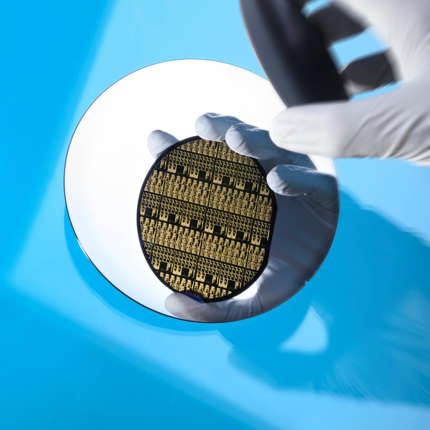
Salience Labs’ technology has been designed from first principles for volume manufacture and is currently fabricating with production-level foundries using standard CMOS processes.
Ian Lane, Partner, Cambridge Innovation Capital states: ‘Salience Labs brings together deep domain expertise in photonics, electronics and CMOS manufacture. Their unique approach to photonics delivers an exceedingly dense computing chip without having to scale the photonics chip to large sizes.’
Alexis Zervoglos, Partner, Oxford Science Enterprises added: ‘Salience Labs offers a pioneering yet pragmatic solution to the widening gap between AI processing demand and semiconductor industry supply. By leveraging photonics in a novel way, Salience Labs is set to make unprecedented advances in compute, transforming existing AI applications and opening up new addressable horizons.’