Semiconductor packaging: from concept to commercialisation
Semiconductor packaging encases integrated circuits in a protective form factor to fit into a device, allowing the chip to be connected to the circuit board. It is an essential part of semiconductor design and manufacture, yet moving from concept to full-scale packaging presents a number of challenges. Whether you’re a photonics start-up with a great idea or an established company looking to prototype a new design, this white paper outlines the challenges faced from semiconductor package design and prototyping, through process development and optimisation to ensure that your device can be manufactured with the desired throughput and quality.
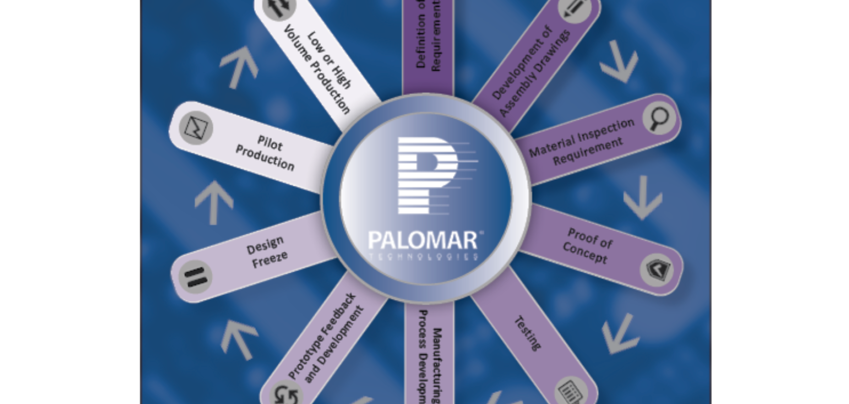
The journey from concept to full-scale semiconductor packaging is often hindered by a number of different obstacles along the way including everything from diverse teams scattered across the world to simply not understanding how the manufacturing process of die bonding, wire bonding or vacuum reflow impacts the package design and vice versa. In this article, the challenges faced from semiconductor package design and prototyping, through process development and process optimisation are presented to ensure the device can indeed be manufactured with the desired throughput and quality.