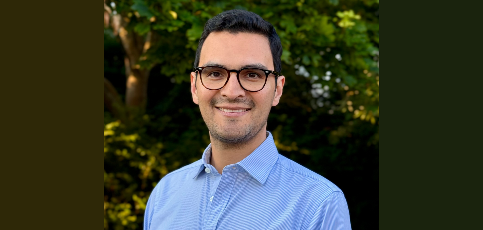
Ruy Sebastian Bonilla

Ruy Sebastian Bonilla’s proudest moment was demonstrating, for the first time, that it is possible to controllably embed ionic charge in dielectric nanolayers to engineer surface and interface properties in silicon devices.
This discovery, later patented, opened a new research field around ‘charged dielectrics’ that has since influenced solar photovoltaics, nanoelectronics, and even emerging quantum devices.

Register for FREE to keep reading
Join 15,000+ photonics professionals staying ahead with:
- Exclusive insights, funding alerts & market trends
- Curated newsletters and digital editions
- Access to The Photonics100 list of R&D champions
- Exclusive panels & roundtables for professional development
- Technical White Papers & product updates to guide smarter decisions
Sign up now
Already a member? Log in here
Your data is protected under our privacy policy.


