Last month, our honorees identified the big cross-industry issues that they think will affect photonics in 2023. In this month’s special feature, we ask them to identify some of the solutions they hope to reach in the year ahead.
Photonics in space/astrophotonics
Prof Ernesto Ciaramella, of the Scuola Superiore Sant’Anna University: “In intra-satellite optical wireless communications, we plan to further shrink our prototypes and make them more flexible, to support different protocols for the onboard equipment communications. Everything that goes on a satellite must be deeply tested and be space-qualified, but we are already making plans to send prototypes on real satellites, for tests that should demonstrate the robustness.”
Peter Kean, R&D Director at G&H: “Our challenges are looking at how to increase the optical power handling of optical amplifiers in the vacuum of space and produce powerful, reliable amplifiers for operation in space. The amplifiers required are significantly higher power than traditional earth-based amplifiers because of the huge distances that need to be covered between satellites and from ground to space!”
Berhanu Bulcha, Research Engineer, Nasa: “Maturing photonics device-based THz spectrometers for flight missions requires funding resources and I think it will continue to be a source of challenge in the near future.”
Iain McKenzie, Senior Photonics Engineer at the European Space Agency: “Developing commercial optical terminals that will offer scalable solutions for satellite constellations.”
Nemanja Jovanovic, Lead Instrument Scientist, Caltech: “The biggest challenge in astrophotonics over the next decade in my opinion is the efficient integration with detectors and scaling to high pixel counts. Multi-pixel detectors are extremely costly and have a form factor mismatch with the output of integrated photonic circuits. Developing approaches to efficiently route the light from planar circuits to multi-pixel arrays will enable the realisation of integrated instruments.”
Medical photonics
Jennifer Kehlet Barton, Professor of Biomedical Engineering, Director of BIO5 Institute, University of Arizona: “In the longer term, the biggest challenge will be to ensure that the medical optics equipment we design provides not only better care to the patient, but a true value to the healthcare system, by saving years of life and/or improving quality of life without adding undue cost.”
Juergen Popp, the Chair for Physical Chemistry and Scientific Director at the Friedrich-Schiller University and Leibniz Institute of Photonic Technology: “A great challenge in the coming years will be simplifying and shortening the path of technological innovations into clinical routine. Translating biophotonic research results faces major challenges, especially with regard to, for example, the EU Medical Device Regulation (MDR) for translational research. Currently, the regulation makes it significantly more difficult or impossible to test biophotonic approaches on patients in the form of preclinical or clinical studies. Numerous photonic technologies have proven their potential for certain diagnostic and therapeutic questions in proof-of-principle studies, but the performance has not yet been demonstrated under routine clinical conditions in the form of comparative studies on a large cohort. Here, funding for such validation studies is urgently needed to generate a marketable product.”
Nicolas Bourg, the CTO of Abbelight: “In single molecule localisation microscopy… the biggest challenge will be to image live cells.”
Optical communications
Polina Bayvel, Professor of Optical Communications & Networks at UCL: “[Designing] adaptive, intelligent low-delay, ultrawideband optical networks for the cloud and the devices needed to achieve this.”
Julie Sheridan Eng, CTO, Coherent: “In datacom, one of the biggest challenges will be making the advances needed in optical components on the timeline the industry needs them. These are serious physics advances to get to 200Gbps.
“I can remember when people were saying they didn’t think a VCSEL could operate above 10Gbps, or a DML above 20Gbps. There were also a lot of non-believers that EMLs could achieve uncooled performance, which has since been demonstrated “So, we are already achieving speeds and performance that people thought unachievable just a few years ago. But we need to keep innovating at a dramatic pace to keep up with the growth in bandwidth demand.”
Dr Maxim Kuschnerov, Director of R&D, Huawei Technologies: “We are deeply engaged in future optical access networks and have begun taking the first steps towards optical fixed infrastructure for the 6G wireless network generation. Indoor wireless access is likely to disrupt beyond Wi-Fi and open up the opportunity for future hybrid optical/wireless networks. We expect first results for future indoor networking in this domain in 2023, which could change the whole paradigm of indoor communication.”
Haik Mardoyan, Senior Research Scientist at Nokia Bell Labs: “Network infrastructure at the service of technological advances, such as eliminating latency on communications between robots and doctors during patient operations in hospitals.”
David Welch, Chief Innovation Officer, Infinera: “Working with the network architects to ensure the extraction of the full value that can come from a point to multi point system [of] optical transceivers through frequency domain modulation of digitally generated subcarriers.”
Peter Winzer, CTO, Nubis Communications: “The biggest challenge is the tight array integration of many parallel system components. In short-reach transceivers, we are no longer talking about a single-fibre pair, we are talking about eight-fibre pairs. Soon, we will be talking about 16- and 32-fibre pairs. In the design of advanced ML/AI engines, we are no longer talking about a single chip with electrical I/O interfaces, we are talking about multi-chiplet processors. Soon, we will be talking about co-packaged optical I/O chiplets. In long-haul transport, we are no longer talking about a single wavelength interfaces, we are talking about superchannels of many wavelengths to carry the interface rate of a logical router port. Soon, we will be talking about an entire long-haul fibre’s worth of capacity as a logical channel, and wavelength switching will be replaced by space switching. In order to make all of the above happen at low power and low cost, massive array integration is needed. A huge challenge, but an unavoidable one.”
Imaging
Jan Bogaerts, CTO, Gpixel: “For each sensor development, we need to find the best trade-off to achieve certain sensor features, using available technologies or based on process advancements that can be realised along the sensor development, and within a given project budget and time schedule. Since 3D stacking brings new degrees of freedom into the design, it creates new opportunities for additional features, increased on-chip processing and bandwidth, and so on.
“However, it also makes the sensor architecture and design process more complex, and thus brings challenges in terms of balancing all these parameters while keeping realistic project schedules.”
Neveen Hosny, Head of Operations and Product Development, M Squared Life: “The advent of light-sheet technology [is] providing fast three-dimensional imaging on a scale that computational technology is already struggling with.
“Light sheet imaging is facing the same issue that super-resolution first saw: ‘look at all this data! but how do we go about analysing it?’. Tools to process data are now the slowest part of light sheet imaging.”
Thomas Kalkbrenner, Team lead & Lead architect Product Line Special 3D, Carl Zeiss Microscopy: “Data management – biomedical 3D imaging creates huge datasets, at the same time many imaging modalities (such as superresolution imaging) require processing of the raw data – ideally in real time.”
Tapani Ryhänen, CTO, Emberion: “Scaling up the production of nanomaterial-based image sensors requires effort and investment. Stability of the image sensors based on nanomaterials will improve gradually. Image sensors that are robust over time and in challenging operating conditions will be created.”
Alexander Braun, Professor of Physics, University of Applied Sciences Düsseldorf: “Linking and correlating optical features [relevant for autonomous driving] to the actual AI performance. Physical-realistic simulation of environmental influences on image quality (temperature, dirt, rain, …).”
Silicon photonics/PICs
June Sang Lee, PhD student, University of Oxford: “It is still challenging to overcome the limitation of large device footprints. While the size of photonic chip itself is reduced to extreme spatial scale (e.g. subwavelength-sized), the size of optical setup, such as lasers, microscope, or spectrometer, cannot be easily reduced or integrated with other photonic components.”
Mayur Kumar Chhipa, Lecturer, Isbat University, Kampala, Uganda: “Photonic circuit modelling is a challenge, particularly since there isn’t a widely accepted Simulation Tools equivalent for modelling and simulating complex optical signals.”
Nicholas Harris, CEO, Lightmatter: “Laser solutions and fibre packaging costs hold the silicon photonics industry back.”
Frank Smyth, CTO, Pilot Photonics: “Continuing to scale coherent optical transceiver bandwidth is becoming increasingly challenging. High-end transceivers currently operate around 90-120Gbaud, and there are efforts underway to reach up to 200Gbaud. But it is getting more and more challenging due to signal integrity issues, and the sheer cost and investment required to switch to new silicon nodes, and design ever faster DSPs. The industry will need to move to multi-wavelength transceivers and we believe that combs are the most effective way to do so.”
Luc Augustin, CTO, SMART Photonics: “Full monolithic integration of high-speed coherent transceivers, including >100Gbaud modulators and narrow linewidth lasers to be able to meet requirements for low-power, low-cost, small-form factor pluggable modules.”
Sensing & metrology
Hanieh Fattahi, Independent group leader/ PI, Max Planck Institute for the Science of Light: “Field-resolved detection at simultaneously higher sensitivity and bandwidth is a big challenge. There have been many field-resolved methodologies, suggested and developed over the past few years. However, they are limited in terms of bandwidth and sensitivity.”
Gabriella Gardosi, Research Associate, Aston Institute of Photonic Technologies: “The commercial fabrication of microphotonic devices with picometre precision will be a significant challenge.”
Matthias Budden, CEO, WiredSense: “One targeted goal is to make broadband pyroelectric detectors useful for beyond 200kHz repetition rates.”
Lasers
Laura Gemini, Group Manager, nanoscale laser processing & health applications, ALPhANOV: “[The biggest challenge will be] for ultrafast technology to reach a readiness level where it becomes competitive to be integrated in high-tech manufacturing lines, with respect to costs and process throughputs. To achieve this goal, it will be essential to achieve fibre transport of high average power (>100sW) ultrafast laser for manufacturing of complex 3D parts while keeping all laser beam properties steady and stable to fit industrial needs. In parallel, the development of robotic positioning systems that can guarantee high movement speed at the same time as high positioning precision and repeatability will be imperative.”
Amy J.R. Bauer, Principal Applications Scientist, Ocean Insight Applied Systems: “The key to implementation of any new measurement application seems to be adequate preparation of the input materials and proper presentation of them to the measurement system. The use of LIBS is no exception to this general rule. This community is used to presenting materials for processing on a conveyor belt, for example, and this may not be optimal for all recycling processing schemes.”
Tim Kunze, CEO, Fusion Bionic: “The next big development is the upscaling of the average laser power (for laser manufacturers) and improved beam delivery technologies (technology providers) to meet the demands of large-area surface processing. [The challenge will be] the upscaling of the laser infrastructure while and, at the same time, addressing the application and process requirements.”
Simonette Pierrot, Principal Laser Engineer, Lumentum Switzerland: “Moving to mass production is a challenge in any industry, the industrial laser field is no exception. Laser system architectures have to be simplified while maintaining their cutting-edge performance, to ensure cost-effectiveness, robustness and manufacturability. Introducing automation and AI is an interesting path forward to help achieve the highest standards of reproducibility and quality.”
Quantum photonics
Dr Reto Häring, Senior Vice-President R&D, Toptica Photonics: “The big question in quantum computing is whether we manage to solve ‘real-world applications’. That means not only that a challenge can be solved but also that it is economically attractive. That makes the difference between a promising technology and a solution.”
Peter Kean, R&D Director, G&H: “Challenges are around improving the performance of our optical components and devices to meet the needs of the quantum community. For example, our acousto-optic modulator product (FibreQ), will need to be modified to have both an incredibly high extinction ratio and much broader tunablity, such that it can enable quantum devices based on trapped ions. This work is now underway and we are developing the techniques to ensure such performance improvements can be measured.”
Pascale Senellart, Scientific Advisor, Quandela: “For scaling up quantum computing and for the development of quantum networks, our next big challenge is the development of efficient sources of highly entangled multiple photons. We have just demonstrated a first proof of concept generation of three-particle entanglement at high rate. Our challenge is now to bring the number of entangled photons and quantum fidelity up.”

Optics
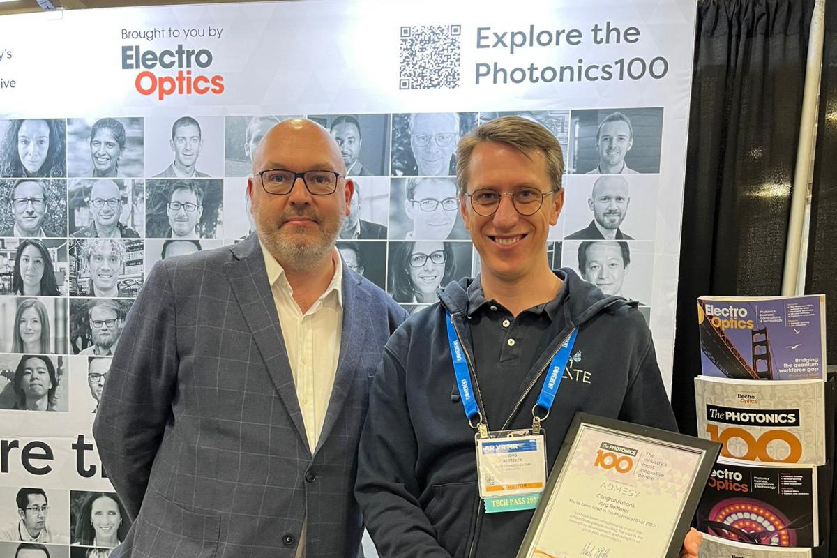
Jörg Reitterer, CTO, TriLite Technologies: “The biggest challenge for consumer AR is to develop next-generation optical architectures that satisfy the requirements of all-day wearable and daylight-bright devices in terms of size, weight, image quality, and power consumption. While AR deployment in enterprise applications is accepted, to a large degree, by trading off some of these requirements, this trade-off is not accepted in the consumer market.”
Lieven Penninck, CEO, PlanOpSim: “I think we are on the brink of large-scale application. Two major challenges need to be overcome for this. The first is identifying winning applications where meta-surfaces can realise their promise of game changing components. Second is industrialising from small scale prototyping to high-volume manufacturing. Both are formidable tasks, but I’m confident these will be overcome by the R&D community in the coming years.”
Nathalie Vermeulen, Professor/PI, Brussels Photonics (B-PHOT), Vrije Universiteit Brussel (VUB): “As the material types are becoming more ‘exotic’ (think about, e.g., low-dimensional materials, metamaterials, …), it becomes increasingly complex to adequately characterise the material nonlinearities. In response to this challenge, I had the opportunity to collaborate with nonlinear-optics pioneer Professor Eric Van Stryland (CREOL) and 20 other experts in the field to provide an overview of recently investigated nonlinear-optical materials and their properties and to list ‘best practices’ for properly measuring, analysing and reporting nonlinearities. Another important challenge, dating back to the early days of nonlinear optics, is to find the right balance between maximising the nonlinear response and minimising optical losses. This trade-off strongly influences the practical applicability of nonlinear-optical devices, and this in turn will determine the overall impact that the field will have on modern society.”
Stefan M. Weber, CEO, Phaseform: “I see three different challenges [in wavefront correction and adaptive optics (AO)]. First, the hardware must become customisable and affordable; second, the integration of adaptive optic components into optical systems must be seamless; and, third, the user experience must be right, meaning the technology must become virtually invisible to the end customer: microscopy users.”


